SLVUBY5A March 2021 – July 2021 TPSM63603
1 EVM Setup
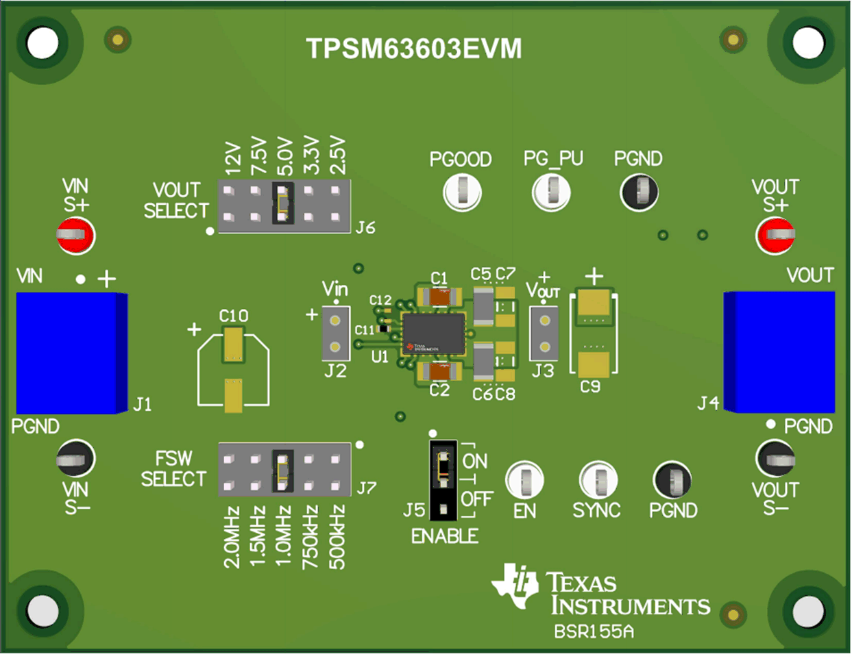
Figure 1-1 highlights the user interface items associated with the EVM. The VIN Power terminal block (J1) is used for connection to the host input supply and the VOUT Power terminal block (J4) is used for connection to the load. These terminal blocks accept up to 16-AWG wire.
 Figure 1-1 EVM User Interface
-
Use the VIN S+ and VIN S- test points along with the VOUT S+ and VOUT S- test points located near the power terminal blocks as voltage monitoring points where voltmeters can be connected to measure VIN and VOUT. Do not use these S+ and S- monitoring test points as the input supply or output load connection points. The PCB traces connecting to these test points are not designed to support high currents.
-
Use the VIN scope (J2) and VOUT scope (J3) test points to monitor VIN and VOUT waveforms with an oscilloscope. These test points are intended to use un-hooded scope probes outfitted with a low inductance ground lead (ground spring) mounted to the scope probe barrel. The two sockets of each test point are on 0.1-in centers. Connect the scope probe tip to the top socket labeled "+" and connect the scope ground lead to the bottom socket.
- The control test points located near the top and bottom of the EVM test the features of the device. Refer to the Section 2 section for more information on the individual control test points.
-
The VOUT SELECT jumper (J6) is provided to select the desired output voltage: 2.5 V, 3.3 V, 5.0 V, 7.5 V, or 12 V. Before applying power to the EVM, make sure that the jumper is present and properly positioned for the intended output voltage. Always remove input power before changing the jumper settings.
-
The FSW SELECT jumper (J7) is provided to select the desired switching frequency: 500 kHz, 750 kHz, 1.0 MHz, 1.5 MHz, or 2.0 MHz. Before applying power to the EVM, make sure that the jumper is present and properly positioned for the intended switching frequency. Always remove input power before changing the jumper settings.
- The device can be turned on or off using the enable jumper (J5). Place the jumper in the ON position to enable the device. Place the jumper in the OFF position to disable the device. The undervoltage lockout (UVLO) can be set by populating resistors R1 and R2 located on the bottom side of the EVM. Refer to the data sheet for recommended UVLO resistor values. The SYNC test point is provided for a convenient location to connect a clock signal. The power good (PGOOD) test point is available to monitor when a valid output voltage is present on the EVM. Additionally, the PG_PU pin is present as a convenient point to connect a pullup voltage for the PGOOD signal.