SLVUC00
September 2020 – MONTH
1
Introduction
1.1
Description
1.2
Features
2
Electrical Performance
3
Schematic
4
Layout
4.1
Setup (Channel 1 / Channel 2)
4.1.1
J1, TP2 / J7, TP8 – Input Connections
4.1.2
J2, TP4 / J6, TP7 – Output Connections
4.1.3
J5, TP5 / J10, TP13 – ON
4.1.4
TP3/TP9 - VIN Sense, TP1/TP6 – VOUT Sense
4.1.5
J11, TP10 – VBIAS
4.1.6
J4 / J9 – Output capacitor (Optional)
4.1.7
TP11, TP12 – GND
5
Operation
6
Test Configurations
6.1
On-Resistance (RON) Test Setup
6.2
Rise Time Test Setup
7
Bill of Materials (BOM)
3
Schematic
Figure 3-1
illustrates the TPS22976AEVM schematic.
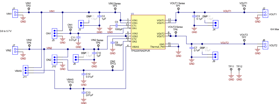
Figure 3-1
TPS22976AEVM Schematic