SLVUC02B September 2020 – May 2021 TPSM41615 , TPSM41625
2 Getting Started
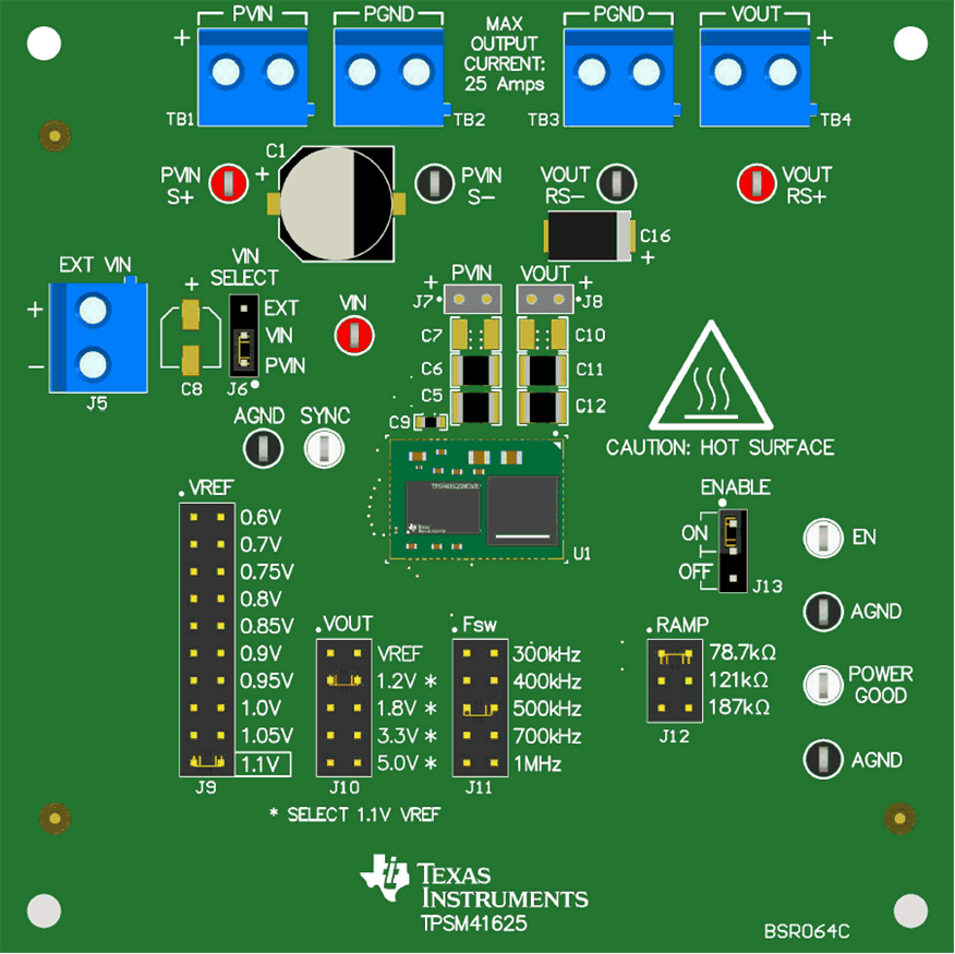
Figure 2-1 highlights the user interface items associated with the EVM. The PVIN and PGND terminal blocks (TB1 and TB2) are used for connection to the host input supply and the VOUT and PGND terminal blocks (TB3 and TB4) are used for connection to the load. These terminal blocks can accept up to 16-AWG wire.
 Figure 2-1 EVM User Interface
The PVIN S+ and PVIN S- input voltage test points as well as the RS+ and RS- output voltage test points, located near the power terminal blocks are intended to be used as voltage monitoring points where voltmeters can be connected to measure PVIN and VOUT. Do not use these S+ and S- monitoring test points as the input supply or output load connection points. The PCB traces connecting to these test points are not designed to support high currents.
The PVIN Scope (J7) and VOUT Scope (J8) sockets can be used to monitor PVIN and VOUT waveforms with an oscilloscope. These test points are intended for use with un-hooded scope probes outfitted with a low-inductance ground lead (ground spring) mounted to the scope probe barrel. The two sockets of each test point are on 0.1 inch centers. The scope probe tip should be inserted into the socket marked with a "+" sign, and the scope ground lead should be inserted into the other socket.
The control test points located around the device are made available to test the features of the device. Refer to the Test Point Description section for more information on the individual control test points. Other features, such as UVLO (R2, R3), ILIM (R23), SS (R24) and MODE (R25) can be altered by manually adding or changing the value on the associated footprints for each component located on the bottom-side of the EVM.
The VREF jumper (J9), VOUT jumper (J10), FSW jumper (J11), and the RAMP jumper (J12) are provided for selecting the internal reference voltage, switching frequency, desired output voltage, and appropriate RAMP setting. Before applying power to the EVM, make sure that the jumpers are present and properly positioned for the intended output voltage. Ensure to set the internal reference voltage prior to selecting the desired output voltage (selecting the highest reference voltage will result in the most accurate output voltage set point). Refer to Table 2-1 for the recommended jumper settings.
| OUTPUT VOLTAGE | VREF SELECT (J9) | VOUT SELECT (J10) | FSW SELECT (J11)(1) | RAMP (J12) |
|---|---|---|---|---|
| 0.6 V - 0.75 V | 0.6 V - 0.75 V | VREF | 500 kHz - 700 kHz | 187 kΩ |
| 0.8 V - 0.95 V | 0.8 V - 0.95 V | VREF | 500 kHz - 1 MHz | 78.7 kΩ |
| 1 V - 1.1 V | 1 - 1.1 V | VREF | 400 kHz - 1 MHz | 187 kΩ |
| 1.2 V | 1.1 V | 1.2 V | 400 kHz - 1 MHz | 187 kΩ |
| 1.8 V | 1.1 V | 1.8 V | 400 kHz - 1 MHz | 187 kΩ |
| 3.3 V | 1.1 V | 3.3 V | 400 kHz - 1 MHz | 78.7 kΩ |
| OUTPUT VOLTAGE | VREF SELECT (J9) | VOUT SELECT (J10) | FSW SELECT (J11)(1) | RAMP (J12) |
|---|---|---|---|---|
| 0.6 V - 0.95 V | 0.6 V - 0.95 V | VREF | 500 kHz - 700 kHz | 78.7 kΩ |
| 1 V - 1.1 V | 1 - 1.1 V | VREF | 700 kHz - 1 MHz | 78.7 kΩ |
| 1.2 V | 1.1 V | 1.2 V | 500 kHz - 1 MHz | 121 kΩ |
| 1.8 V | 1.1 V | 1.8 V | 500 kHz - 700 kHz | 187 kΩ |
| 3.3 V | 1.1 V | 3.3 V | 700 kHz - 1 MHz | 187 kΩ |
| 5.0 V | 1.1 V | 5.0 V | 700 kHz - 1 MHz | 187 kΩ |
For example, if an output voltage of 1.8 V is desired and is supplied by a 12-V input, then a proper configuration is as follows:
- Set VREF (J9) as 1.1 V.
- Set VOUT (J10) as 1.8 V.
- Select FSW (J11).
- Set RAMP (J12) as 187 kΩ.
Another example, if an output voltage of 1.0 V is desired and is supplied by a 12-V input, then a proper configuration is as follows:
- Set VREF (J9) as 1.0 V.
- Set VOUT (J10) as VREF.
- Select FSW (J11).
- Set RAMP (J12) as 78.7 kΩ