SLVUC03 November 2022
5.2 Jumper Configuration
This section describes the configuration of main jumpers. You can configure the jumpers according to your application.
J1 NTC Header
The J1 header is used to verify the thermal foldback function. The NTC pin actually detects the voltage of external NTC circuit, it can be connected to thermistor(NTC or PTC) divider or NTC_VAR. NTC_VAR is the output of TPL0102, which is a I2C digital potentiometer. If you are sure what type of thermistor to be used on your system, you can put the thermistor and resistor divider on our EVM board to test the thermal foldback function. If you can use I2C to control the output of TPL0102, you can connect to NTC_VAR.Or you can directly apply an external voltage to NTC contact pin without any jumper. The thermistor assembled on the EVM is positive temperature coefficient(PTC).
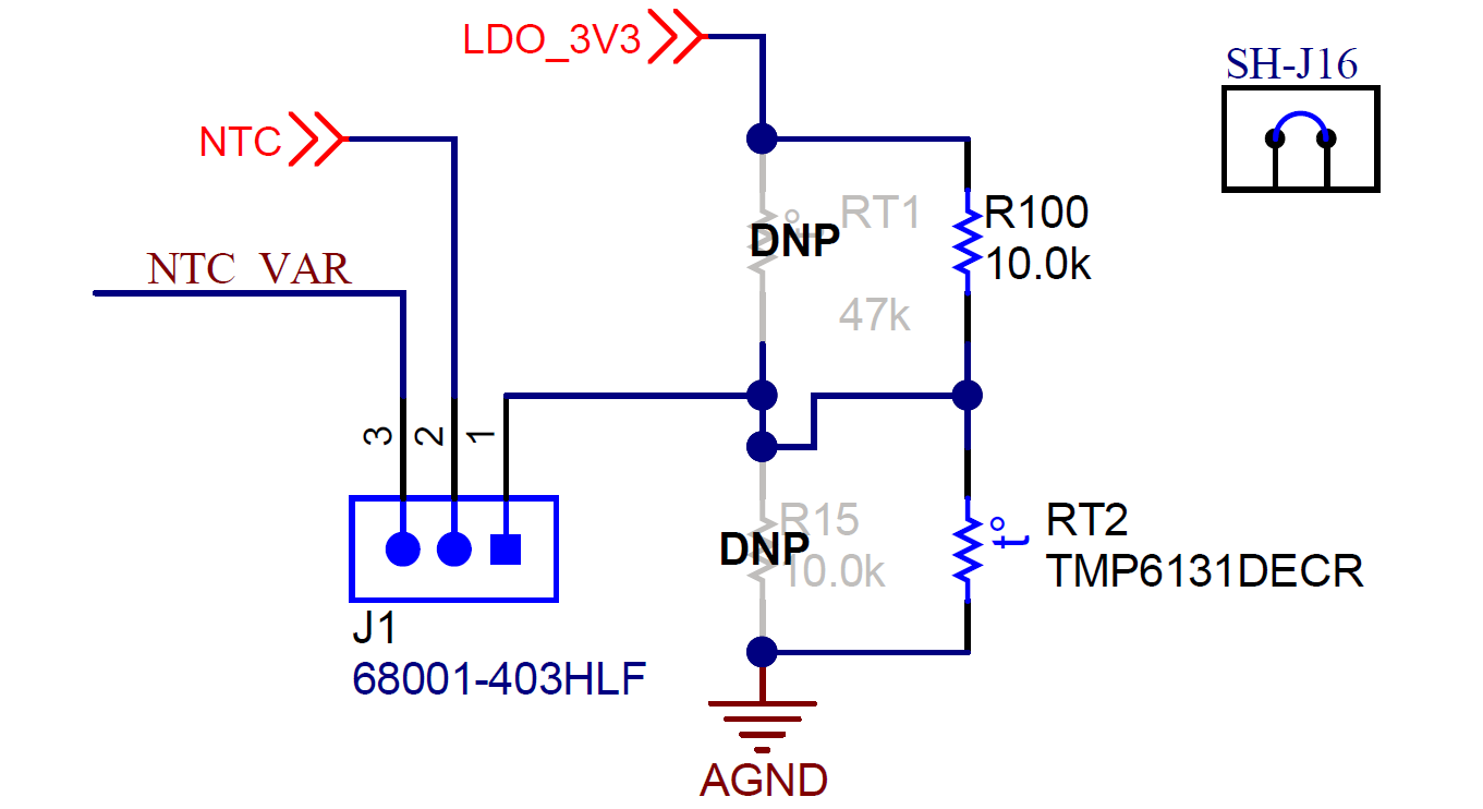 Figure 5-1 J1 NTC Header
J6 I2C MUX
This header expands the I2C1 connections of TPS25762/72-Q1: it can connect to GPIO expander, I2C temperature sensor and EEPROM. Since I2C bus can support multiple slaves, it is recommended to connect all pins.
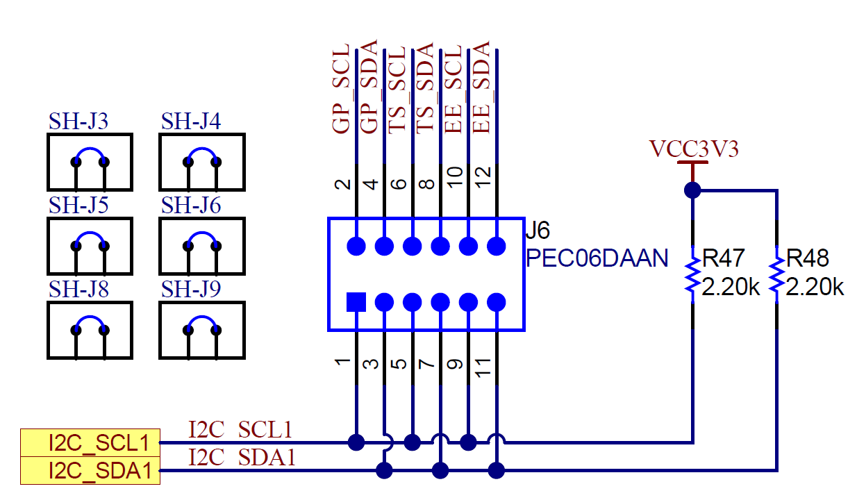 Figure 5-2 J6 I2C MUX
J7 TVSP Connector
In order to support USB connector pin short to VBUS or VBAT protection, it is recommended to connect an RC circuit on TVSP pin as shown in Figure 5-4 .
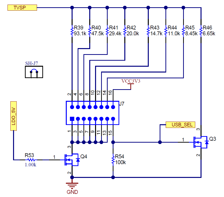 Figure 5-3 J7 TVSP Connector
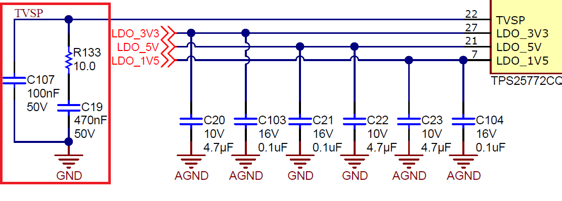 Figure 5-4 TVSP Damper Network
J8 USB2ANY Connector, J9 I2C MUX, and J10 Aardvark Connector
J8 and J10 are the I2C connectors for USB2ANY and Aardvark tools. J9 is I2C mux for USB2ANY and Aardvark. The I2C from USB2ANY or Aardvark can be configured to connected to I2C1, I2C2, and I2C3. Since I2C bus can support multiple slaves, it is recommended to connect all pins.
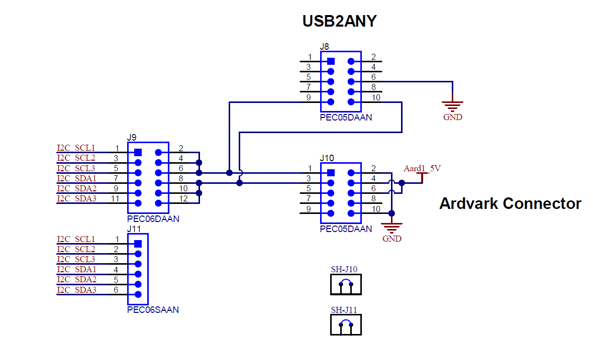 Figure 5-5 Connectors and MUX for USB2ANY
and Aardvark
Figure 5-5 Connectors and MUX for USB2ANY
and AardvarkJ14 External VCONN and Auxiliary Power Enable Connector
J14 is used to choose VCONN source and enable external 5 V, 3.3 V and 1.1 V auxiliary power. 3.3 V and 1.1 V voltage are power source of HUB and TIVA. To make sure the EVM board have full function, we recommend connecting all pins of J14. Schematic is shown in Figure 6-5
J15 DITH/SYNC Connector
J15 is dithering or synchronous selector for TPS55288-Q1. DITH/SYNC pin can be configured to connect to C75 to set a dithering frequency or connect to TPS25762/72-Q1 SYNC output to synchronize the switching frequency.
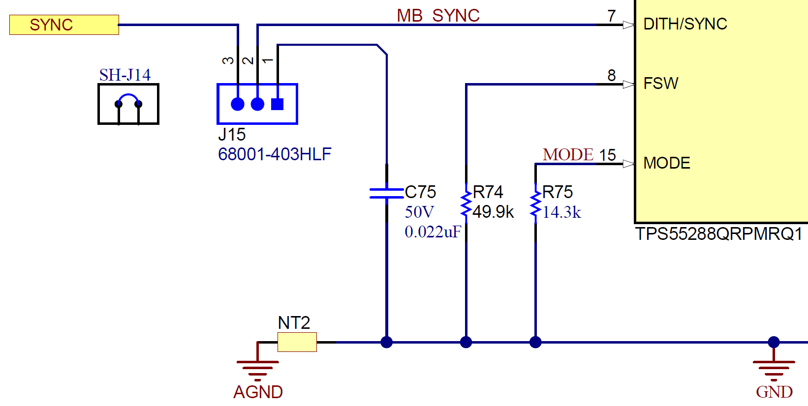 Figure 5-6 J15 DITH/SYNC
Connector
Figure 5-6 J15 DITH/SYNC
ConnectorJ18/J19 GPIO9 configuration
J18 and J19 is used to configure the GPIO9 according to the function of GPIO9 pin.J18 is the header used to configure GPIO9 as an interrupt I/O for I2C. J19 is the header used to configure GPIO9 as an enable signal or discharge signal for Port B.
 Figure 5-7 J18/J19 GPIO9
Configuration
Figure 5-7 J18/J19 GPIO9
ConfigurationJ20 Enable Signal for TPS55288-Q1
J20 is the header to configure the enable signal of TPS55288-Q1. The default enable signal is the 3.3V LDO from TPS25772-Q1. It can be configured to GPIO9 or external enable signal as needed.
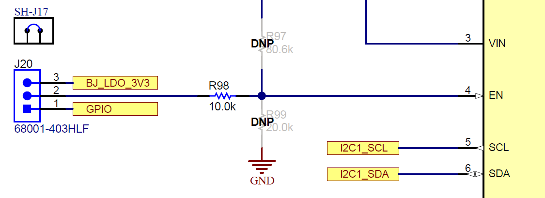 Figure 5-8 J20 Enable Signal for
TPS55288-Q1