SLVUC07A December 2020 – May 2021 TPS543320
- Trademarks
- 1Introduction
- 2Configurations and Modifications
-
3Test Setup and Results
- 3.1 Input/Output Connections
- 3.2 Efficiency
- 3.3 Output Voltage Regulation
- 3.4 Load Transient and Loop Response
- 3.5 Output Voltage Ripple
- 3.6 Input Voltage Ripple
- 3.7 Synchronizing to a Clock
- 3.8 Start-up and Shutdown with EN
- 3.9 Start-up and Shutdown with VIN
- 3.10 Hiccup Current Limit
- 3.11 Overvoltage Protection
- 3.12 Thermal Performance
- 4Board Layout
- 5Schematic and Bill of Materials
- 6Revision History
3.11 Overvoltage Protection
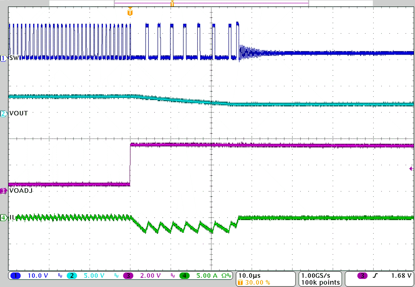
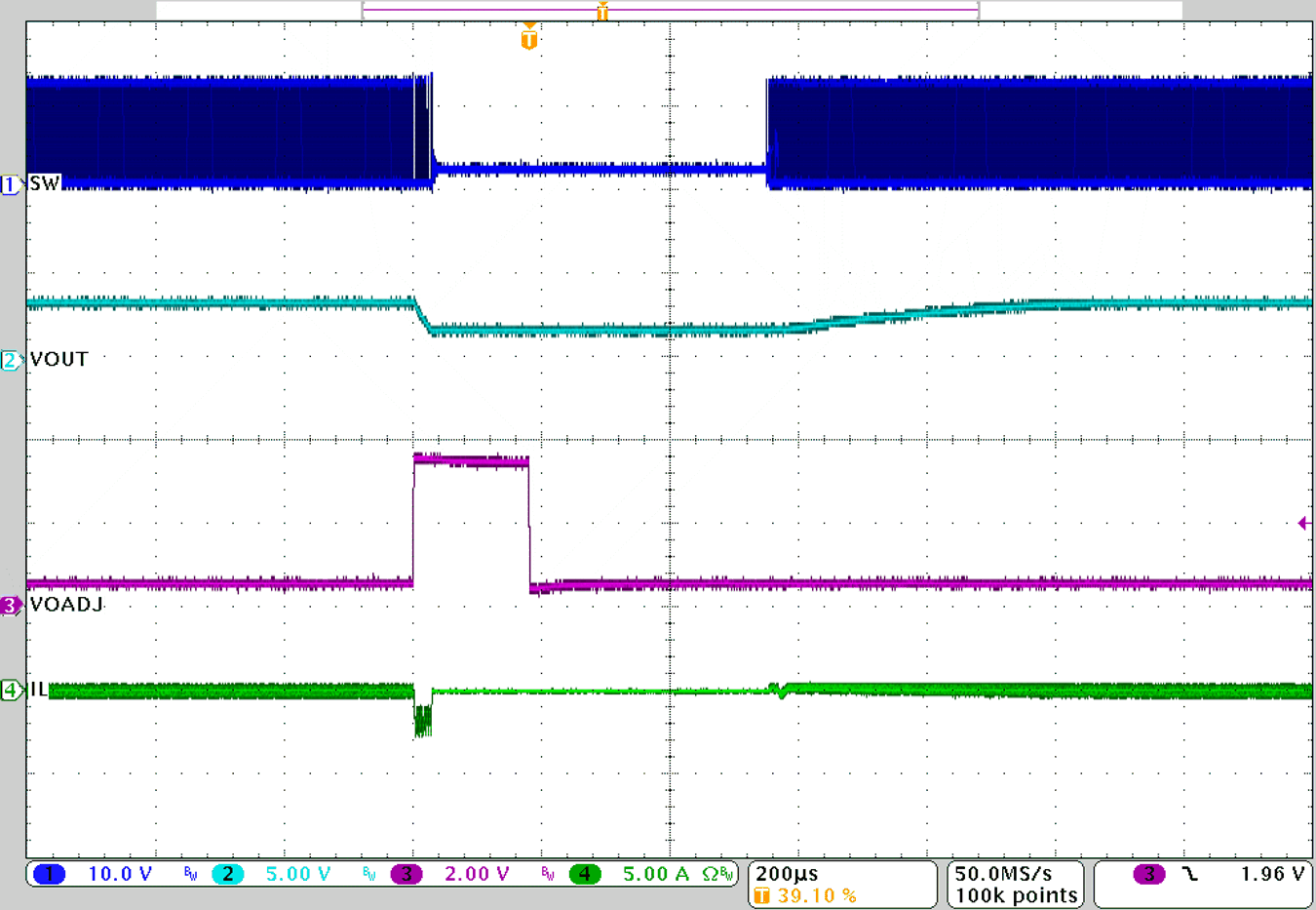
Figure 3-32 and Figure 3-33 show the overvoltage protection behavior of U2. This is tested by applying a step to the FB pin with a function generator through the VO_ADJ test point. The VO_ADJ test point is initially equal to the reference voltage of 0.5 V and is stepped up to 3.3 V. The TPS543320 attempts to restart immediately after the OVP fault is cleared. It does not wait for the hiccup time period.
 Figure 3-32 U2 Overvoltage
Protection
 Figure 3-33 U2 OVP and Recover