SLVUC07A December 2020 – May 2021 TPS543320
- Trademarks
- 1Introduction
- 2Configurations and Modifications
-
3Test Setup and Results
- 3.1 Input/Output Connections
- 3.2 Efficiency
- 3.3 Output Voltage Regulation
- 3.4 Load Transient and Loop Response
- 3.5 Output Voltage Ripple
- 3.6 Input Voltage Ripple
- 3.7 Synchronizing to a Clock
- 3.8 Start-up and Shutdown with EN
- 3.9 Start-up and Shutdown with VIN
- 3.10 Hiccup Current Limit
- 3.11 Overvoltage Protection
- 3.12 Thermal Performance
- 4Board Layout
- 5Schematic and Bill of Materials
- 6Revision History
5.1 Schematic
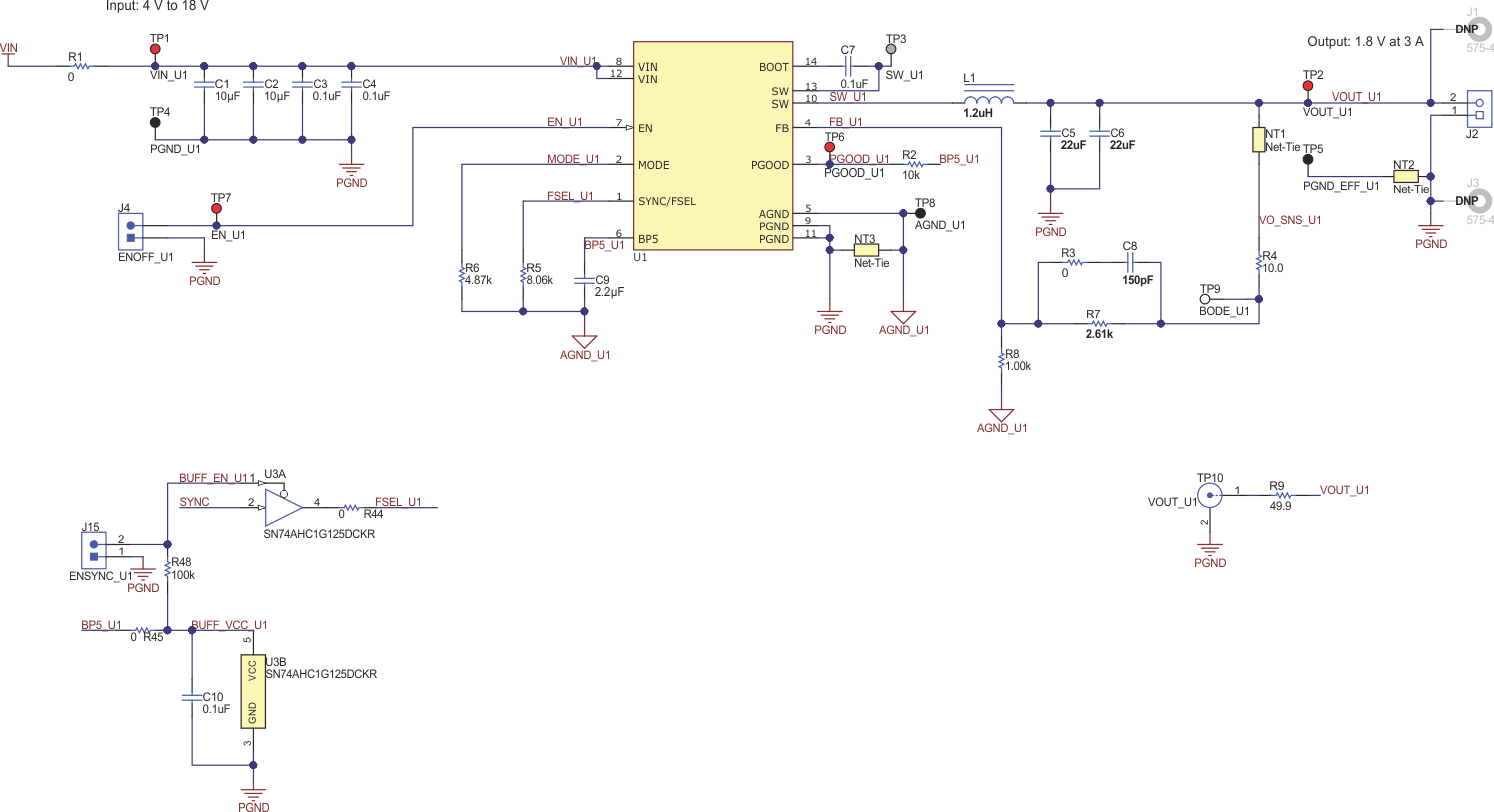
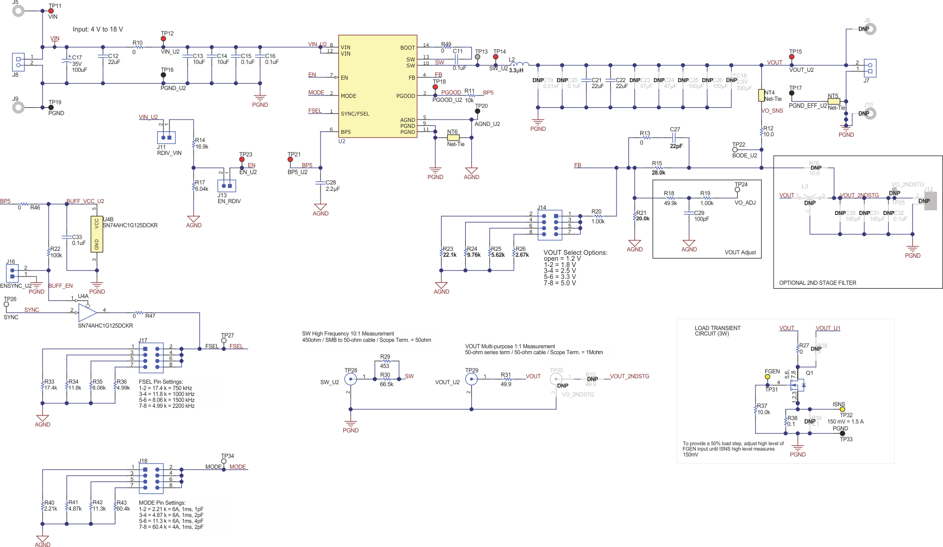
Figure 5-1 is the schematic for U1. Figure 5-2 is the schematic for U2.
 Figure 5-1 U1
Schematic
 Figure 5-2 U2 Schematic