SLVUC22 July   2021 TPS62912 , TPS62913


  1.   Trademarks
  2. 1Introduction
    1. 1.1 Performance Specification
    2. 1.2 EVM Features and Modifications
      1. 1.2.1 Input and Output Capacitors
      2. 1.2.2 Enable Level Shifter and Adjustable Threshold Voltage
      3.      Power Good Level Shifter
      4. 1.2.3 NR/SS Capacitor
      5. 1.2.4 Feedforward Capacitor
      6. 1.2.5 S-CONF Resistor
      7. 1.2.6 Loop Response Measurement
      8. 1.2.7 Single LC Filter Operation
  3. 2Setup
    1. 2.1 Input/Output Connector Descriptions
    2. 2.2 Ripple Measurement
  4. 3Test Results
  5. 4Board Layout
  6. 5Schematic and Bill of Materials
    1. 5.1 Schematic
  7. 6Bill of Materials

Board Layout

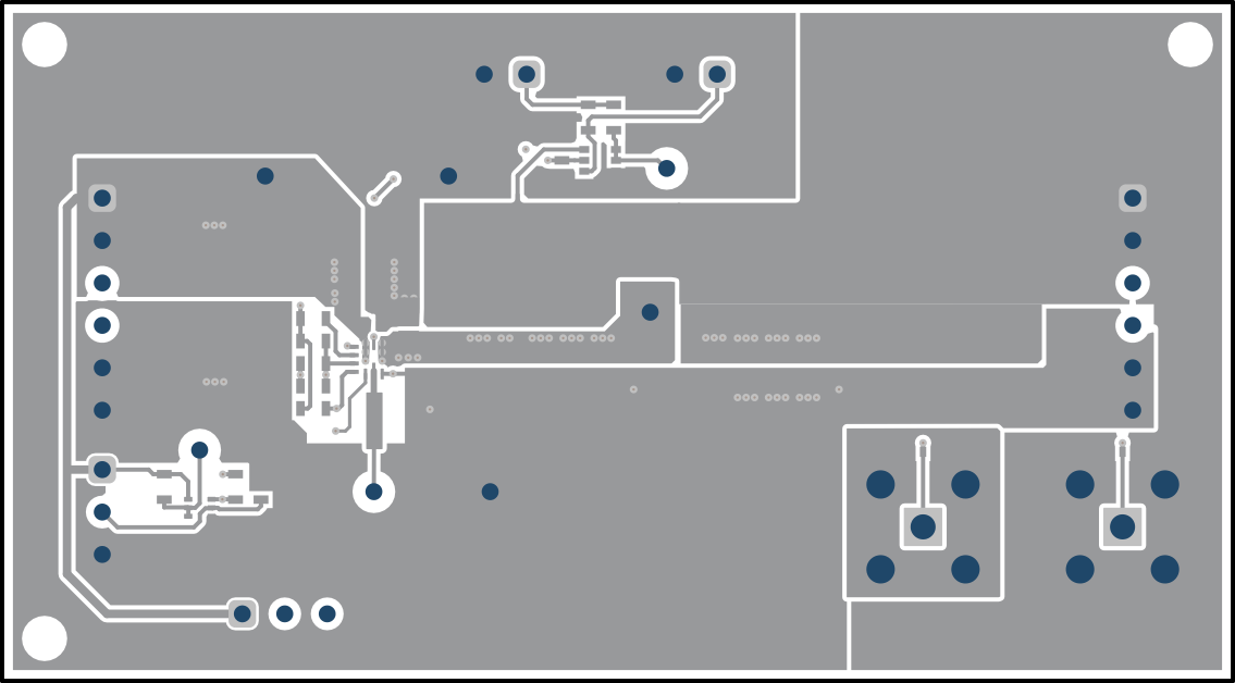
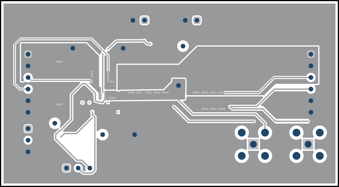
This section provides the EVM board layout and illustrations in Figure 4-1 through Figure 4-6. The Gerbers are available on the EVM product page.

GUID-20210528-CA0I-VD3C-CD2M-ZDD9Z5W33L5C-low.gif Figure 4-1 Top Assembly
GUID-20210528-CA0I-9Z1K-BWHH-N95WVRMLF98F-low.gif Figure 4-2 Top Layer
GUID-20210528-CA0I-H2Q1-88B6-8C5QDDMH8PDM-low.gif Figure 4-3 Internal Layer 1
GUID-20210528-CA0I-WF6M-TLJC-C7XKXVT69CVK-low.gif Figure 4-4 Internal Layer 2
GUID-20210528-CA0I-CGPP-DFRM-8M5DQWMTRNZ5-low.gif Figure 4-5 Bottom Layer
GUID-20210528-CA0I-X49P-LQ5D-MSWFG7Z7NM95-low.gif Figure 4-6 Bottom Layer (Mirrored)