SLVUC43 May 2021 TLVM13630
4 PCB Layouts
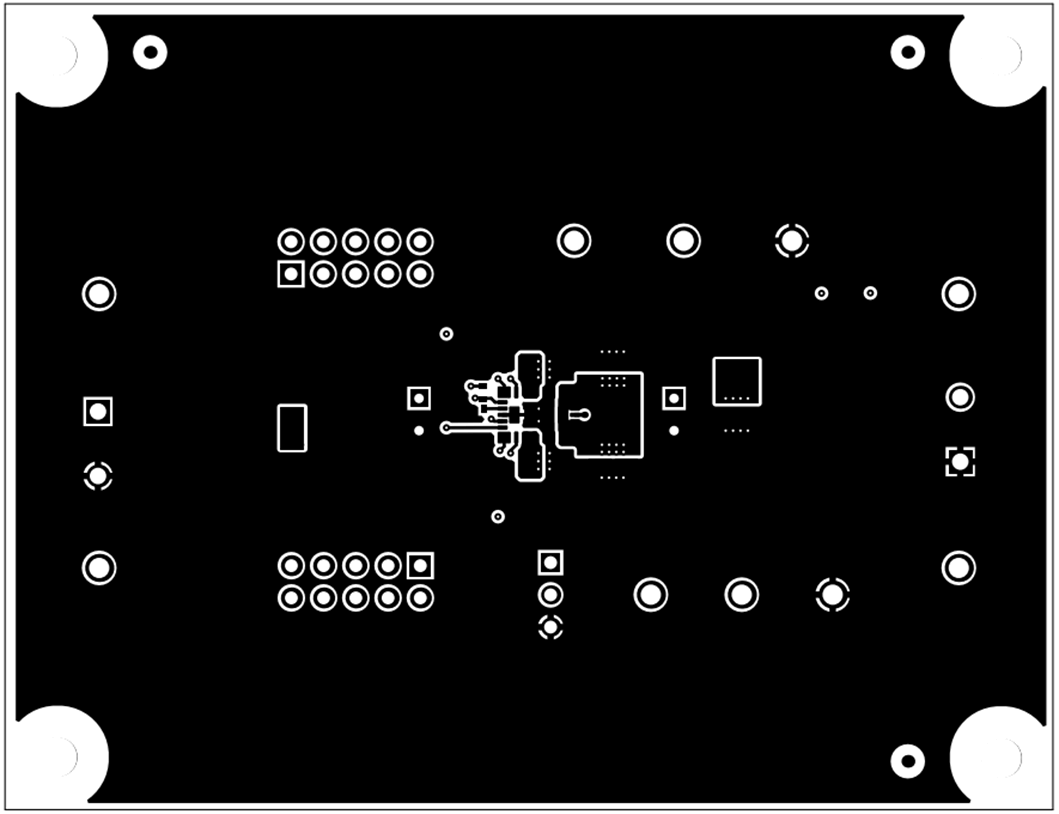
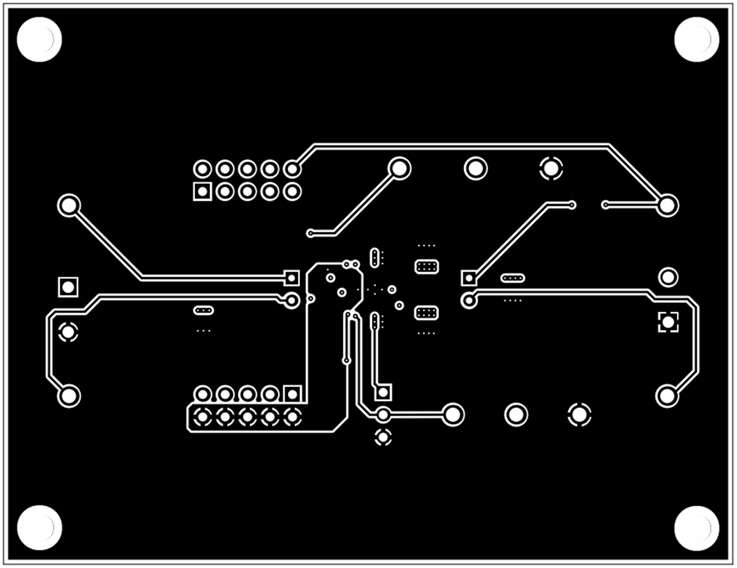
Figure 4-1 through Figure 4-6 show the EVM PCB layout images.
 Figure 4-1 Top Silk Screen (Top View)
 Figure 4-2 Top Copper Layer (Top
View)
 Figure 4-3 Signal Layer 1 (Top View)
 Figure 4-4 Signal Layer 2 (Top View)
 Figure 4-5 Bottom Layer (Top View)
 Figure 4-6 Bottom Layer Silk Screen (Bottom
View)