SLVUCD8 February 2022
4 PCB Layouts
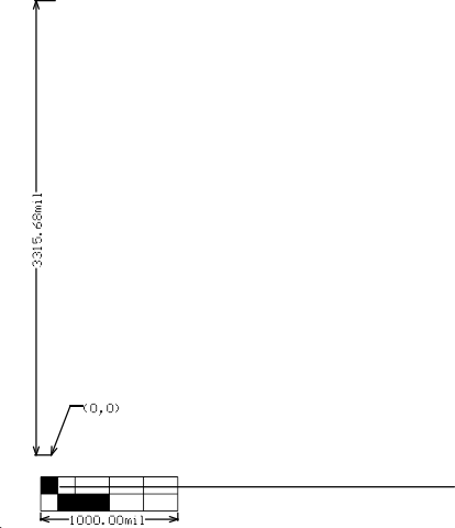
Figure 4-1 through Figure 4-8 show the EVM PCB layout images.
 Figure 4-1 Top Overlay
Figure 4-3 Top Layer

Figure 4-5 Bottom Solder
 Figure 4-7 Drill Drawing
Figure 4-2 Top Solder

Figure 4-4 Bottom Layer

Figure 4-6 Bottom Overlay
 Figure 4-8 Board Dimensions