SLVUCD8 February 2022
2 EVM Setup and Quick Start Guide
Table 2-1 lists the default configuration.
| PARAMETER | SPECIFICATION |
|---|---|
| Input power supply | 4 V to 14 V |
| Operating temperature | 25°C |
| Switching frequency | 500 kHz |
The TPS7H5005/6/7/8EVM can be quickly turned on and run using the connections shown in Table 2-2.
| TERMINAL OR TEST POINT | VOLTAGE SOURCE |
|---|---|
| J11 (VIN) | 4-V to 14-V input at 10 mA. See Positive and Negative Terminal for J11 connections. |
| TP9 (COMP) | 1 V at < 10 mA (input range can be –0.3 V to 3.3 V based on the TPS7H500x-SEP Radiation-Tolerant 2-MHz Current Mode PWM Controllers in Space Enhanced Plastic data sheet). |
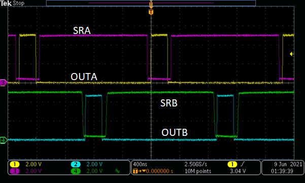
The device should then turn on and operate in open loop mode as shown in Figure 2-1. Figure 2-1 shows the output of TPS7H5005/6/7/8-SP measured on J1–J4 with the quick start method.
 Figure 2-1 TPS7H5005/6/7/8-SEP Output
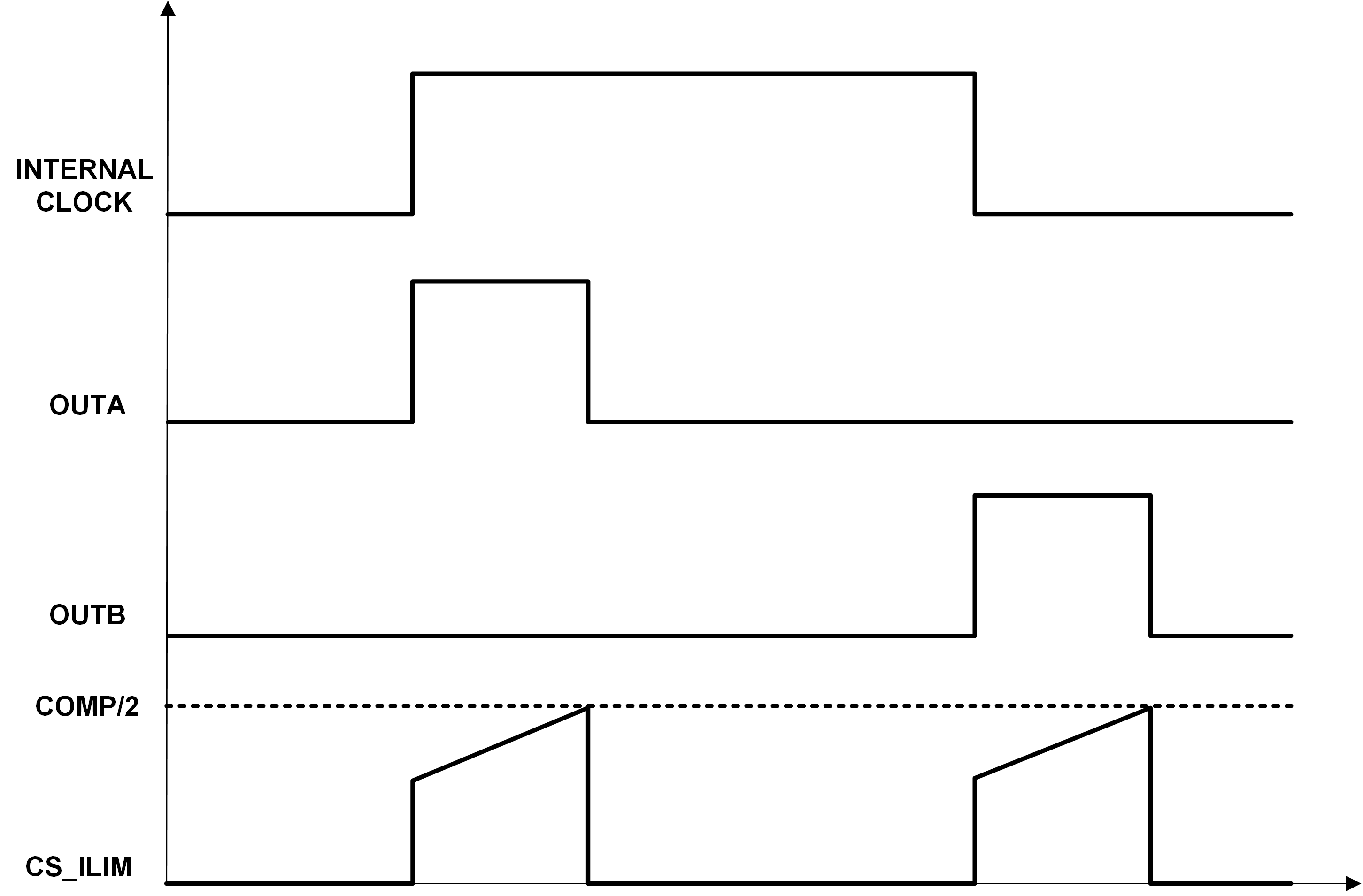
The operation of this mode is such that forcing the voltage on COMP will create an output on the TPS7H5005/6/7/8EVM. The duty cycle varies based on the input voltage on COMP as well as the triangle waveform created by the CS_LIM circuit, or any other waveform that the user decides to add to the CS_LIM pin. See Figure 2-2 for signal generation waveforms. Note that OUTB and SRB will not be present for TPS7H5006EVM, and TPS7H5007EVM. SRA and SRB will not be present for TPS7H5008EVM.
Figure 2-2 shows waveforms for input and output signal generations for the TPS7H5005/6/7/8EVM based on COMP voltage and CS_LIM pin voltage.
 Figure 2-2 Duty Cycle Generation