SLVUCF5A March 2022 – August 2022 DRV8329
4.4 DRV8329AEVM Configurability
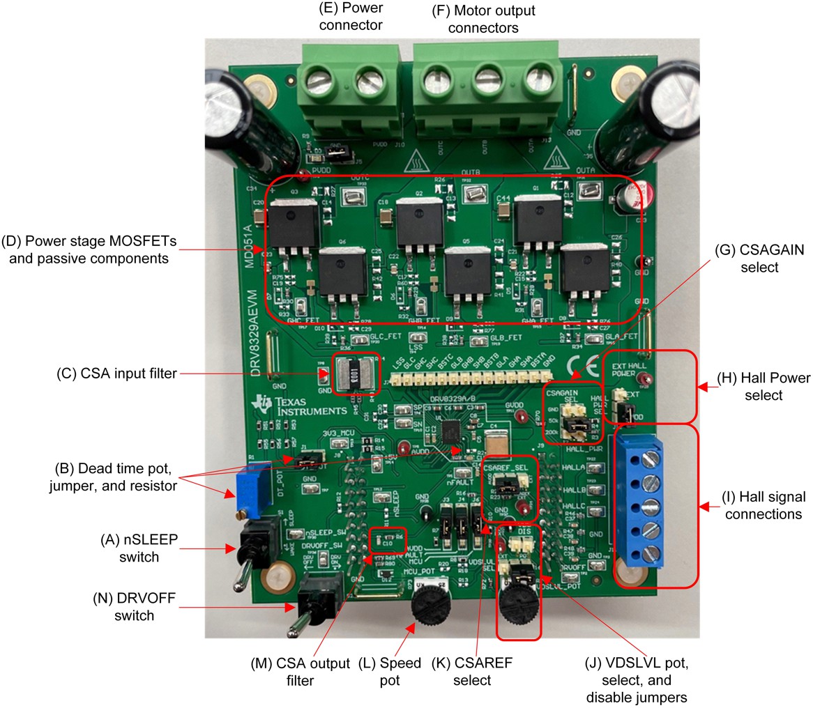
The DRV8329AEVM includes a variety of user-selectable jumpers and unpopulated components on the PCB to choose user settings and evaluate the DRV8329A, DRV8329B, DRV8329C, or DRV8329D device. A summary of those selectable settings is listed in Table 4-2 (defaults in bold) and can be seen on the board in Figure 4-6.
Table 4-2 User-Selectable Jumpers
| Id. | Setting Name | Description | Position | Function |
|---|---|---|---|---|
| A | nSLEEP switch | Places DRV8329 in sleep mode | S2 = Left | Sleep mode |
| S2 = Right | Operating mode | |||
| B | Dead time potentiometer, jumper, & resistor | Jumper to enable dead time control from potentiometer and potentiometer used to set the resistance for DT pin. | J1 = Populated | DT from pot is enabled |
| J1 = DNP | DT from pot is disabled | |||
| R1 (CW = more DT, CCW = less DT) | Sets dead time of gate driver outputs | |||
| R2 | Fixed resistor for DT pin | |||
| C | CSA input filter | Input filter to filter any Vsense switching transients at the current sense amplifier inputs. | R45 = R43 = 0 ohm C30, C31, C32 = DNP | CSA input filtering |
D | Power stage MOSFETs and passive components | Optional passive components for tuning power stage, i.e. series gate resistors, RC snubbers, PVDD-GND capacitors, PVDD-LSS capacitors | R28, R29, R30, R34, R35, R36 = 10 ohm | Series gate resistors (GHA, GHB, GHC, GLA, GLB, GLC) |
| R25/C12, R26/C13, R27/C14, R40/C26, R41/C24, R42/C25 = DNP | RC snubbers (HS FET A, HS FET B, HS FET C, LS FET A, LS FET B, LS FET C) | |||
| C18, C20, C44 = 2.2uF | PVDD-VDRAIN bypass capacitor | |||
| C21, C22, C23 = 0.01uF | PVDD-LSS bypass capacitors | |||
| G | CSA gain select | Selects the gain setting of the integrated CSA in V/V. | J2 = GND | CSAGAIN = 5 V/V |
| J2 = 50 k | CSAGAIN = 10 V/V | |||
| J2 = 200 k | CSAGAIN = 20 V/V | |||
| J2 = DNP | CSAGAIN = 40 V/V | |||
| H | HALL_PWR select | Use J6 to supply Hall power from AVDD or external hall power. | J11 = AVDD | Supplies AVDD to Hall power |
| J11 = EXT | Supply external hall power from EXT HALL POWER test point. | |||
| J | VDSLVL potentiometer, select and disable jumpers | Potentiometer to set VDSLVL between 0.1 ̶ 2.5 V, VDSLVL_SEL to select voltage source, disable jumper to disable VDSLVL | J16 = POT | VDSLVL set from potentiometer |
| J16 = EXT | VDSLVL set from VDS EXT test point | |||
| J15 = Populated | VDSLVL is disabled (100 kΩ to GVDD) | |||
| J15 = DNP | VDSLVL is enabled | |||
| R74 (CCW = higher VDSLVL, CW = lower VDSLVL) | Sets VDSLVL from 0.1 V ̶ 2.5 V | |||
| K | CSAREF select | Jumper to select CSA reference voltage from AVDD or an external reference source. | J14 = AVDD | CSAREF = AVDD |
| J14 = EXT | CSAREF = CSAREF EXT test point | |||
| L | Speed pot | Sets speed of the motor when potentiometer is enabled in the GUI. | R73 (CW = less speed, CCW = more speed) | Sets duty cycle from 0% to 100%. |
| M | External CSA output filter | RC output filter to suppress high frequency transients of CSA output from current shunt. | R59 = 330 ohms, C31 = 470 pF | Fc ~10 MHz |
| N | DRVOFF switch | Turns off the gate driver outputs. | S2 = Down | Drivers are on |
| S2 = Up | Drivers are off (DRVOFF is enabled) |
 Figure 4-6 User-adjustable jumpers, resistors, and switches on DRV8329AEVM