SLVUCK1 April   2024 TPS7H4011-SP


  1.   1
  2.   Abstract
  3.   Trademarks
  4. 1Description
  5. 2Features
  6. 3Evaluation Module Overview
    1. 3.1 Introduction
    2. 3.2 Kit Contents
    3. 3.3 Specification
    4. 3.4 Device Information
  7. 4Hardware
    1. 4.1 Setup
      1. 4.1.1 Jumper Configuration
      2. 4.1.2 Transient Load Circuit
    2. 4.2 Connector Descriptions
    3. 4.3 Best Practices
  8. 5Implementation Results
    1. 5.1 Default Configuration Results
    2. 5.2 Soft Startup
    3. 5.3 Voltage Ripple on VOUT
    4. 5.4 Load Step
    5. 5.5 Frequency Response
  9. 6Hardware Design Files
    1. 6.1 Schematics
    2. 6.2 PCB Layouts
    3. 6.3 Bill of Materials (BOM)
  10. 7Compliance Information
  11. 8Related Documentation

Voltage Ripple on VOUT

Note: To avoid coupled noise from the switch node, output voltage ripple was measured across C24 using a "tip-and-barrel" method with a coil wire ground.
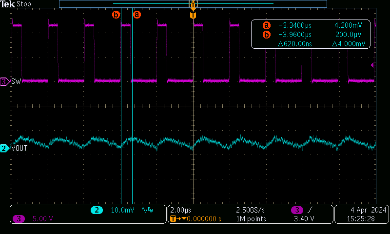
GUID-20240404-SS0I-LNLX-JQHL-3LFP4FLTB76Q-low.pngFigure 5-2 Output Voltage Ripple