SLVUCO4 October   2023 TPS62916


  1.   1
  2.   TPS62916EVM Evaluation Module
  3.   Trademarks
  4. 1Introduction
    1. 1.1 Performance Specification
    2. 1.2 Modifications
      1. 1.2.1 Input and Output Capacitors
      2. 1.2.2 Configurable Enable Threshold Voltage
      3. 1.2.3 NR/SS Capacitor
      4. 1.2.4 Feedforward Capacitor
      5. 1.2.5 S-CONF Resistor
      6. 1.2.6 Loop Response Measurement
      7. 1.2.7 Single LC Filter Operation
  5. 2Setup
    1. 2.1 Input and Output Connector Descriptions
    2. 2.2 Ripple Measurement Setup
  6. 3 Test Results
  7. 4 Board Layout
  8. 5Schematic and Bill of Materials
    1. 5.1 Schematic
  9. 6Bill of Materials

Ripple Measurement Setup

The extremely low noise and low ripple levels of the TPS62916 necessitate a low-noise test setup for accurately measuring the output voltage ripple. Use the SMA connectors, J1 and J2, to measure the output voltage ripple, before and after the second LC filter. Do not use a normal 10x oscilloscope probe with a high-impedance termination to the oscilloscope. Instead, connect the SMA connector directly to the oscilloscope with a coaxial (coax) cable through a DC blocker. A DC blocker enables the use of the smallest V/div setting on the oscilloscope to view the ripple. To prevent noise pickup and block reflections on the coax cable, the oscilloscope must be set to full bandwidth (BW) and DC coupling with a 50-Ω termination.

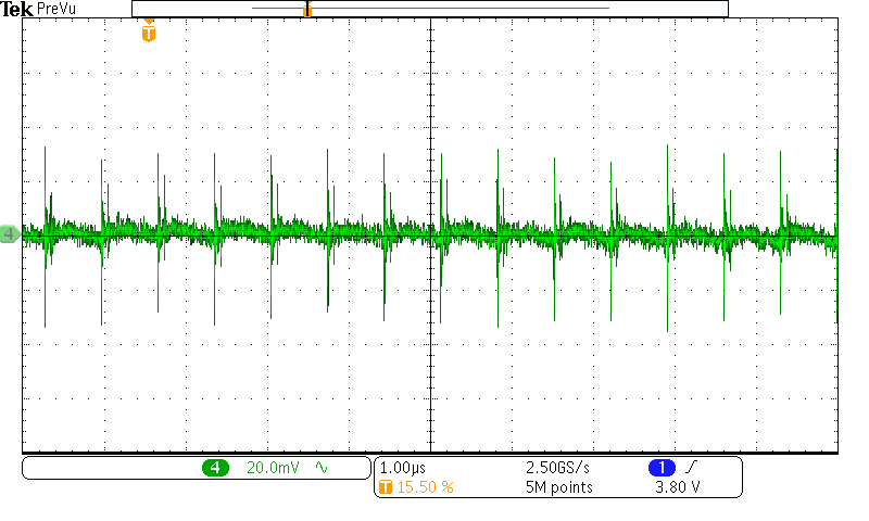
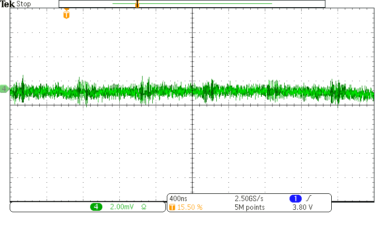
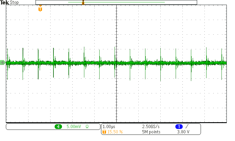
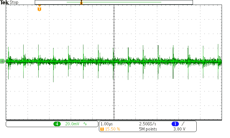
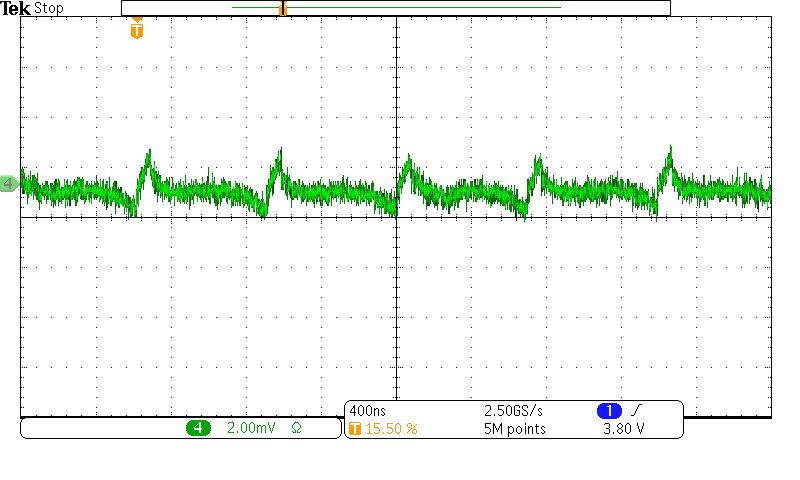
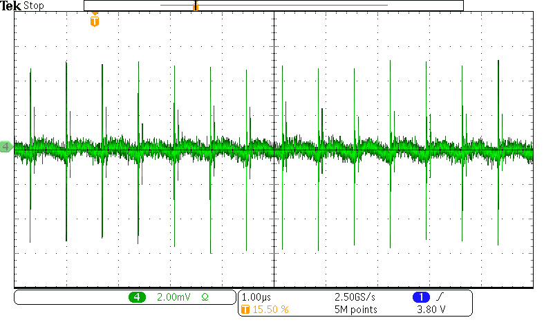
Figure 2-1 and Figure 2-4 show the correct measurement settings and output voltage ripple result, while Figure 2-2, Figure 2-3, Figure 2-5, and Figure 2-6 show common measurement methods and settings that cannot accurately measure the very low output voltage ripple.
GUID-6F2B7FC3-D175-44D2-8D35-F2E34B8A12BE-low.png
VIN = 12 V, VOUT = 1.2 V, IOUT = 6 A, JP2 Open, Full BW, DC Coupling, 50-Ω Termination With DC Blocker
Figure 2-1 Output Voltage Ripple, Measured at J1
GUID-F4A7E43C-6491-46F2-BD90-8271966AF840-low.png
VIN = 12 V, VOUT = 1.2 V, IOUT = 6 A, JP2 Open, Full BW, DC Coupling, 50-Ω Termination With DC Blocker
Figure 2-2 Output Voltage Ripple, Measured Across C10 With 1x Probe
GUID-A00FB0EA-B1A1-4761-AF0F-8827BFE51420-low.png
VIN = 12 V, VOUT = 1.2 V, IOUT = 6 A, JP2 Open, Full BW, AC Coupling, High-Impedance Termination Without DC Blocker
Figure 2-3 Output Voltage Ripple, Measured Across C10 With 10x Probe
GUID-19279C4F-17D6-4FFB-AF7A-0A11A344FF0D-low.png
VIN = 12 V, VOUT = 1.2 V, IOUT = 6 A, JP2 Open, Full BW, DC Coupling, 50-Ω Termination With DC Blocker
Figure 2-4 Output Voltage Ripple, Measured at J2
GUID-DB375D14-82FF-45A1-A396-5C7024C22613-low.png
VIN = 12 V, VOUT = 1.2 V, IOUT = 6 A, JP2 Open, Full BW, DC Coupling, 50-Ω Termination With DC Blocker
Figure 2-5 Output Voltage Ripple, Measured Across C19 With 1x Probe
GUID-B7DDC7ED-57B7-4611-8752-7C4AB5EF12AF-low.png
VIN = 12 V, VOUT = 1.2 V, IOUT = 6 A, JP2 Open, Full BW, AC Coupling, High-impedance Termination Without DC Blocker
Figure 2-6 Output Voltage Ripple, Measured Across C19 With 10x Probe