SLVUCS1A july 2023 – august 2023 TPS7H2140-SEP
2.1.1 Connectors
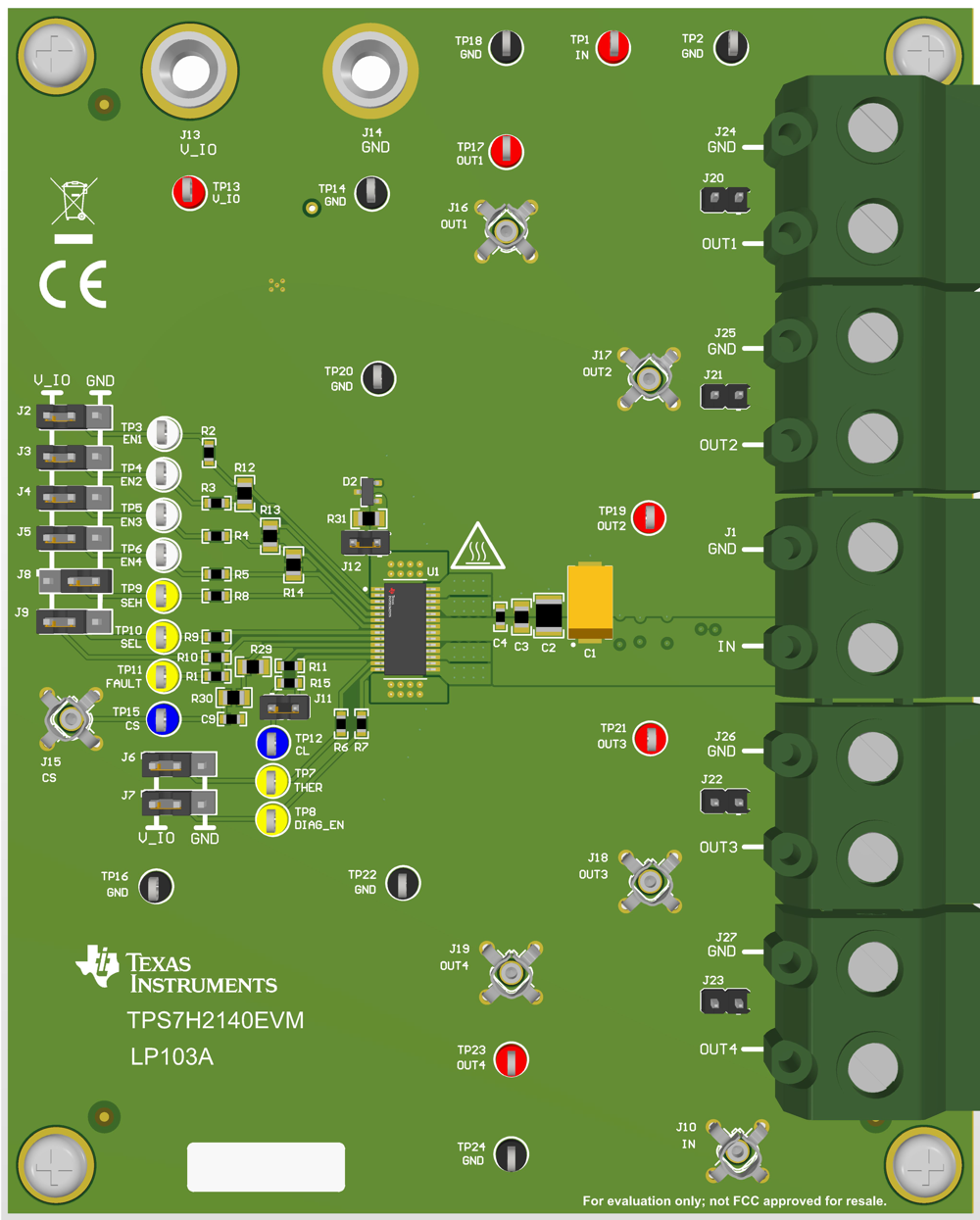
 TPS7H2140EVM
Table 2-1 Summary of Connectors and Test
Points
| Reference Designator | Function | |
|---|---|---|
| J1 (pin 1) | IN | Input voltage and current |
| J1 (pin 2) | GND | |
| J13 | V_IO | Input for IO voltage |
| J14 | GND | |
| J24 (pin 1) | OUT1 | Output voltage and current for channel 1 |
| J24 (pin 2) | GND | |
| J25 (pin 1) | OUT2 | Output voltage and current for channel 2 |
| J25 (pin 2) | GND | |
| J26 (pin 1) | OUT3 | Output voltage and current for channel 3 |
| J26 (pin 2) | GND | |
| J27 (pin 1) | OUT4 | Output voltage and current for channel 4 |
| J27 (pin 2) | GND | |
| TP1, J10 | IN | Test point |
| TP17, J16 | OUT1 | |
| TP19, J17 | OUT2 | |
| TP21, J18 | OUT3 | |
| TP23, J19 | OUT4 | |
| TP2, TP14, TP16, TP18, TP20, TP22, TP24 | GND | |
| TP3 | EN1 | |
| TP4 | EN2 | |
| TP5 | EN3 | |
| TP6 | EN4 | |
| TP7 | THER | |
| TP8 | DIAG_EN | |
| TP9 | SEH | |
| TP10 | SEL | |
| TP11 | FAULT | |
| TP12 | CL | |
| TP15, J15 | CS | |
| J2 | V_IO - EN1 - GND | Shunt for mode selection |
| J3 | V_IO - EN2 - GND | |
| J4 | V_IO - EN3 - GND | |
| J5 | V_IO - EN4 - GND | |
| J6 | V_IO - THER - GND | |
| J7 | V_IO - DIAG_EN - GND | |
| J8 | V_IO - SEH - GND | |
| J9 | V_IO - SEL - GND | |
| J11 | CL - GND | |
| J12 | GND - GND_IC | |
| J20 | Open-load detection pull-up OUT1 | |
| J21 | Open-load detection pull-up OUT2 | |
| J22 | Open-load detection pull-up OUT3 | |
| J23 | Open-load detection pull-up OUT4 | |