SLVUCS2A August 2024 – September 2024 TPS25763-Q1
2.4 Jumper Information
J3 TVSP Jumper
This jumper selects the boot mode and I2C address for TPS25763-Q1.
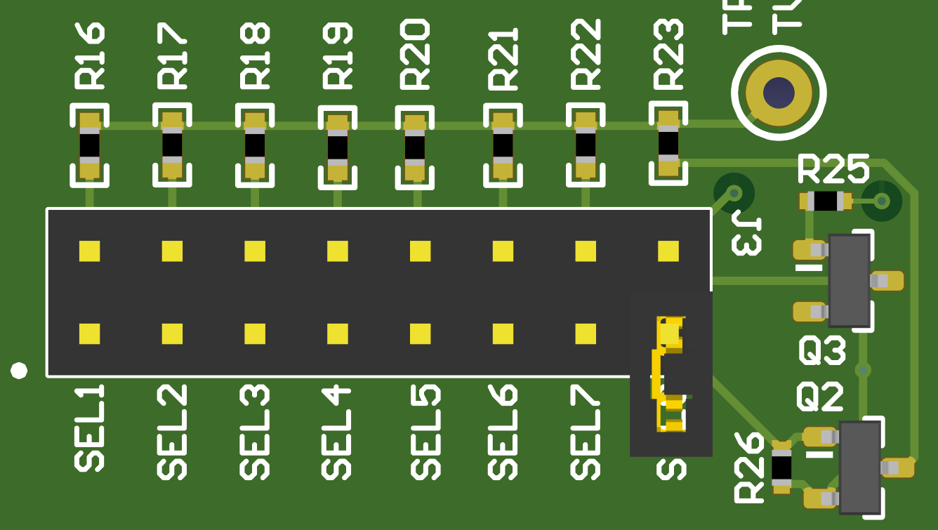 Figure 2-2 J3 TVSP Jumper
See the RTVSP Configuration Settings table in the TPS25763-Q1 Automotive Single USB Type-C Alternate Mode Power Delivery Controller with Buck-Boost Regulator data sheet for selection description.
| Pins | Name | Description |
|---|---|---|
| Open | SEL0 | EEPROM boot. I2C address 0x22. 3.3V logic |
| 1:2 | SEL1 | MCU boot. I2C address 0x23. 3.3V logic |
| 3:4 | SEL2 | EEPROM boot. I2C address 0x22. 1.8V logic |
| 5:6 | SEL3 | MCU boot. I2C address 0x23. 1.8V logic |
| 7:8 | SEL4 | EEPROM boot. I2C address 0x23. 3.3V logic |
| 9:10 | SEL5 | MCU boot. I2C address 0x22. 3.3V logic |
| 11:12 | SEL6 | EEPROM boot. I2C address 0x23. 1.8V logic |
| 13:14 | SEL7 | MCU boot. I2C address 0x22. 1.8V logic |
| 15:16 | SEL8 | Firmware update mode |
J15 Power Supply Control
This jumper is used to disable or select power supplies for the board.
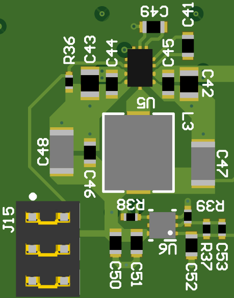 Figure 2-3 J15 Power Supply Control
| Pins | Label | Description |
|---|---|---|
| 1-2 | 5V EN | Enable buck regulator to generate VCC5V |
| 3-4 | 5V-LDO | Connect LDO_5V to VCC5V |
| 5-6 | 3V3 1V1EN | Enable the LDO to generate VCC3V3 and VCC1V1 for MCU |
J8 I2C Connection Jumper
This jumper block expands the I2C1 connections of TPS2573DQ1. The jumper can connect to the I2C temperature sensor and EEPROM. Since I2C bus can support multiple targets, TI recommends to connect all pins.
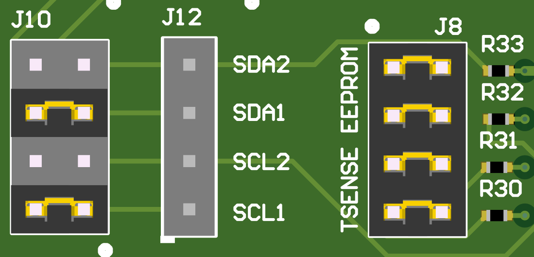 Figure 2-4 J8 I2C Connection Jumper
| Pins | Label | Description |
|---|---|---|
| 1-2 and 3-4 | LM75 Temp Sense | Connect the I2C1 bus of TPS25763-Q1 to LM75 temperature sensor |
| 4-5 and 7-8 | EEPROM | Connect the I2C1 bus of TPS25763-Q1 to the on board EEPROM |
J4 NTC Selection Jumper
The J4 header is used to verify the Thermal Foldback function. The NTC pin detects the voltage of an external NTC circuit. The pin can be connected to a thermistor (NTC or PTC) divider or users can directly apply an external voltage to NTC contact pin without any jumper. The thermistor assembled on the EVM is positive temperature coefficient (PTC).
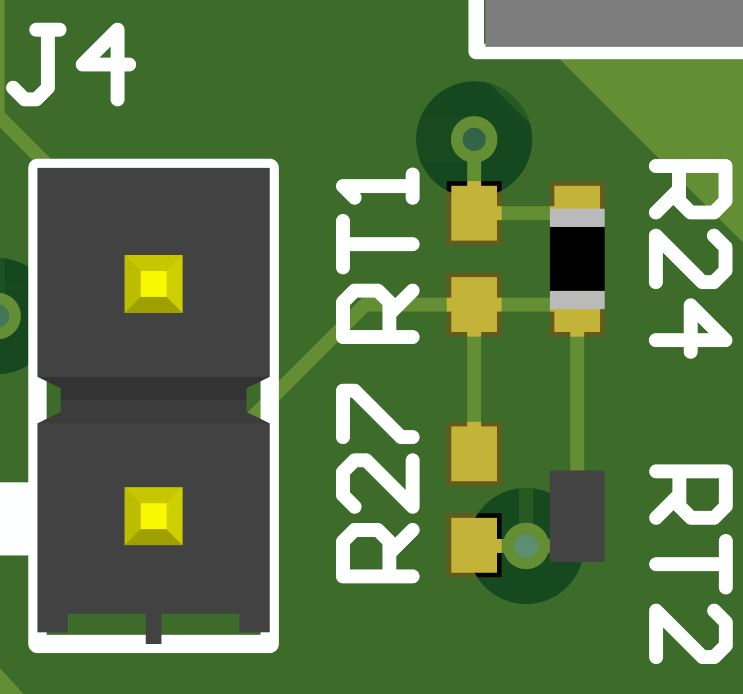 Figure 2-5 J4 NTC Selection Jumper
| Pins | Label | Description |
|---|---|---|
| 1:2 | PTC divider | Connect PTC resistor divider to TPS25763-Q1 NTC pin |
Open | Open | Connect a DC voltage supply to NTC pin to emulate temperature change |
J7 TMP75B-Q1 Alert Connection Jumper
The J7 jumper can be used to test the function of an I2C controlled temperature sensor in place of the NTC/PTC/resistor divider circuit. The temperature feedback is available via I2C or the ALERT signal can directly be connected to the TPS2673-Q1 NTC pin.
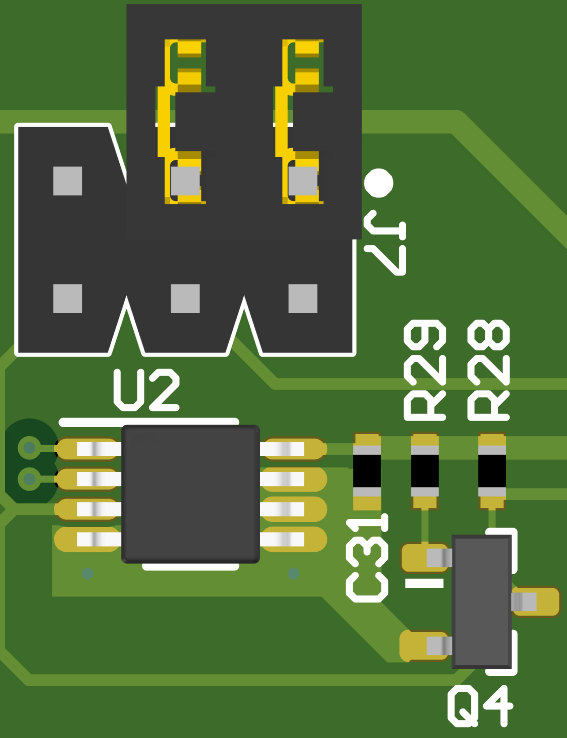 Figure 2-6 J7 TMP75B-Q1 Alert Connection
Jumper
Figure 2-6 J7 TMP75B-Q1 Alert Connection
Jumper| Pins | Description |
|---|---|
| 1:2 | Connect the active low output of TMP75B-Q1 pin to the IRQ1 pin (GPIO9 of TPS25763-Q1) |
| 3:4 | Connect the inverted (active high) output of the Alert pin of TMP75B-Q1 to the NTC pin of TPS25763-Q1 |
| 5:6 | Connect the active low output of the Alert pin of TMP75B-Q1 to the NTC pin of TPS25763-Q1 |
J23, J5, J6, J19, J16, J17 Power Selection Jumpers
Controls whether a given peripheral circuit is powered by VCC3V3 (external LDO) or LDO_3V3 (internal LDO of TPS25763-Q1). This allows users to evaluate whether the system requires an external 3.3V supply. Additionally, a better efficiency measurement of TPS25763-Q1 can be made by removing all Power Selection jumpers.
J21, J20, J22, J1, J2 DisplayPort MUX Configuration Jumpers
Dictates whether TUSB1064 is controlled by TPS25763-Q1 via GPIO signals or I2C commands. The MUX I2C feature is enabled or disabled, then the appropriate signal routing can be made between the MUX and PD controller. If the MUX I2C feature is disabled, then expect the remaining jumpers to be set for GPIO control. Similarly, if the MUX I2C feature is enabled, then expect the remaining jumpers to be set for I2C control.
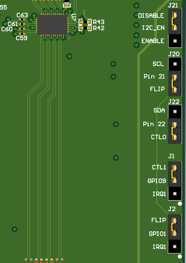 Figure 2-7 DisplayPort MUX Configuration
Jumpers
Figure 2-7 DisplayPort MUX Configuration
Jumpers| Jumper | Label | Description |
|---|---|---|
| J21 | DISABLE | Disable I2C control |
| ENABLE | Enable I2C control | |
| J20 | SCL | MUX pin 21 connected to I2C1 clock signal |
| FLIP | MUX pin 21 connected to FLIP IO signal | |
| J22 | SDA | MUX pin 22 connected to I2C1 data signal |
| CTL0 | MUX pin 22 connected to CTL0 IO signal | |
| J1 | CTL1 | TPS25763-Q1 GPIO9 configured as CTL1 signal |
| IRQ1 | TPS25763-Q1 GPIO9 configured as IRQ1 signal | |
| J2 | FLIP | TPS25763-Q1 GPIO1 configured as FLIP signal |
| IRQ1 | TPS25763-Q1 GPIO1 configured as IRQ2 signal. |
J18 !USB2.0 Data Jumper
Install if USB2.0 data is not required for the system (charge only). This does not impact DisplayPort over USB-C functionality. Installing this jumper causes D+/D- from the Type-C connector to route to TPS25763-Q1 via TS3USB221A-Q1, enabling legacy charging algorithms such as BC1.2.
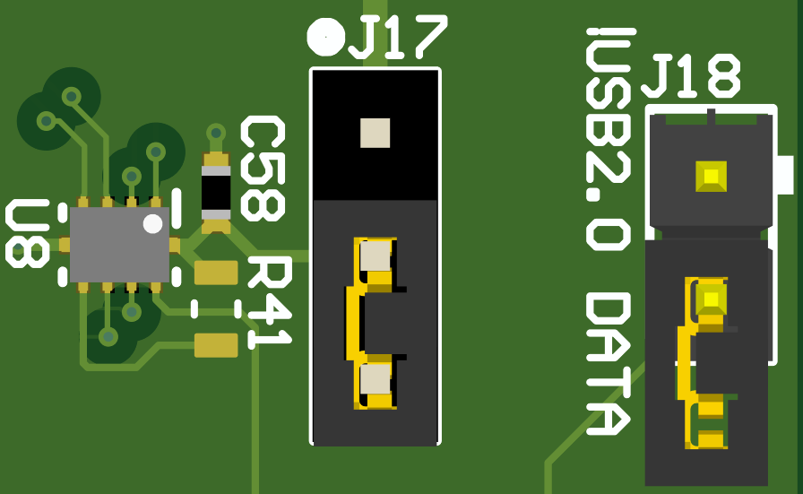 Figure 2-8 !USB2.0 Data Jumper
| Pins | Description |
|---|---|
| 1:2 | USB2.0 data is not passed through to an upstream port. D+/D- from the Type-C receptacle are routed to TPS25763-Q1 for legacy charge handshake capability. |
| Open | USB2.0 data is passed through to upstream port J29. Legacy charge compatibility is unavailable unless implemented in the upstream port. |