SLVUD04 August   2024 TPSM83102


  1.   1
  2.   Description
  3.   Features
  4.   4
  5. 1Evaluation Module Overview
    1. 1.1 Introduction
    2. 1.2 Kit Contents
    3. 1.3 Specification
    4. 1.4 Device Information
  6. 2Hardware
    1. 2.1 Background
    2. 2.2 Setup
    3. 2.3 Input and Output Connectors, Test Points, and Headers Description
      1. 2.3.1 J1, Pin 1 and 2 – VIN
      2. 2.3.2 J1, Pin 3 and 4 – S+/S-
      3. 2.3.3 J1, Pin 5 and 6 – GND
      4. 2.3.4 J2, Pin 1 and 2 – VOUT
      5. 2.3.5 J2, Pin 3 and 4 – S+/S-
      6. 2.3.6 J2, Pin 5 and 6 – GND
      7. 2.3.7 Test Points
        1. 2.3.7.1 TP1, TP2
      8. 2.3.8 Header Information
        1. 2.3.8.1 J4– I2C
      9. 2.3.9 Jumper Information
        1. 2.3.9.1 JP1 – ENABLE
    4. 2.4 Setup
    5. 2.5 Modifications
      1. 2.5.1 IC U1 Operation
  7. 3Software
    1. 3.1 Software Setup
    2. 3.2 Interface Hardware Setup
    3. 3.3 User Interface Operation
      1. 3.3.1 Home Screen
      2. 3.3.2 Settings Screen
      3. 3.3.3 Register Map Screen
    4. 3.4 Register Map
      1. 3.4.1 Register CONTROL1 (Target Address: 0x2A; Register Address: 0x02; Default: 0x08)
      2. 3.4.2 Register VOUT (Target Address: 0x2A; Register Address: 0x03; Default: 0x5C)
      3. 3.4.3 Register CONTROL2 (Target Address: 0x2A; Register Address: 0x05; Default:0x45)
  8. 4Hardware Design Files
    1. 4.1 Schematic
    2. 4.2 Board Layout
    3. 4.3 Bill of Materials
  9. 5Additional Information
    1. 5.1 Trademarks

Home Screen

The Home screen gives a short overview of the TPSM83102 and TPSM83103 devices. To start evaluating the device, click on the Start button or on the Settings or Register Map icons on the left side of the GUI window.
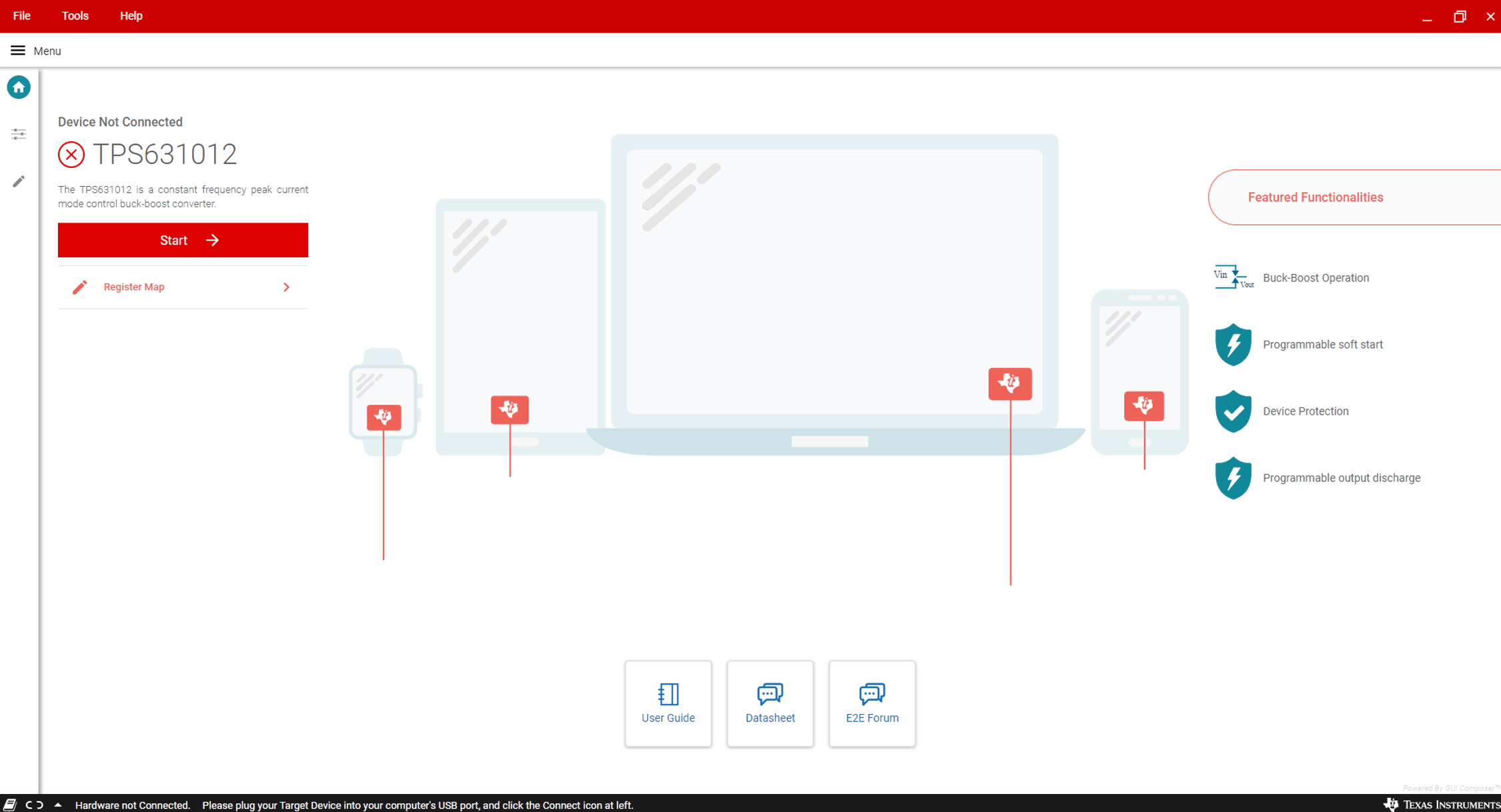
TPSM83102EVM GUI Home ScreenFigure 3-2 GUI Home Screen