SLVUD04 August   2024 TPSM83102


  1.   1
  2.   Description
  3.   Features
  4.   4
  5. 1Evaluation Module Overview
    1. 1.1 Introduction
    2. 1.2 Kit Contents
    3. 1.3 Specification
    4. 1.4 Device Information
  6. 2Hardware
    1. 2.1 Background
    2. 2.2 Setup
    3. 2.3 Input and Output Connectors, Test Points, and Headers Description
      1. 2.3.1 J1, Pin 1 and 2 – VIN
      2. 2.3.2 J1, Pin 3 and 4 – S+/S-
      3. 2.3.3 J1, Pin 5 and 6 – GND
      4. 2.3.4 J2, Pin 1 and 2 – VOUT
      5. 2.3.5 J2, Pin 3 and 4 – S+/S-
      6. 2.3.6 J2, Pin 5 and 6 – GND
      7. 2.3.7 Test Points
        1. 2.3.7.1 TP1, TP2
      8. 2.3.8 Header Information
        1. 2.3.8.1 J4– I2C
      9. 2.3.9 Jumper Information
        1. 2.3.9.1 JP1 – ENABLE
    4. 2.4 Setup
    5. 2.5 Modifications
      1. 2.5.1 IC U1 Operation
  7. 3Software
    1. 3.1 Software Setup
    2. 3.2 Interface Hardware Setup
    3. 3.3 User Interface Operation
      1. 3.3.1 Home Screen
      2. 3.3.2 Settings Screen
      3. 3.3.3 Register Map Screen
    4. 3.4 Register Map
      1. 3.4.1 Register CONTROL1 (Target Address: 0x2A; Register Address: 0x02; Default: 0x08)
      2. 3.4.2 Register VOUT (Target Address: 0x2A; Register Address: 0x03; Default: 0x5C)
      3. 3.4.3 Register CONTROL2 (Target Address: 0x2A; Register Address: 0x05; Default:0x45)
  8. 4Hardware Design Files
    1. 4.1 Schematic
    2. 4.2 Board Layout
    3. 4.3 Bill of Materials
  9. 5Additional Information
    1. 5.1 Trademarks

Register Map Screen

The Register Map screen shows a register-wise view of all parameters. Here, single registers can be read or written to the device (if applicable). Refer to Section 3.4 for a detailed description of the TPSM83102 and TPSM83103 registers.
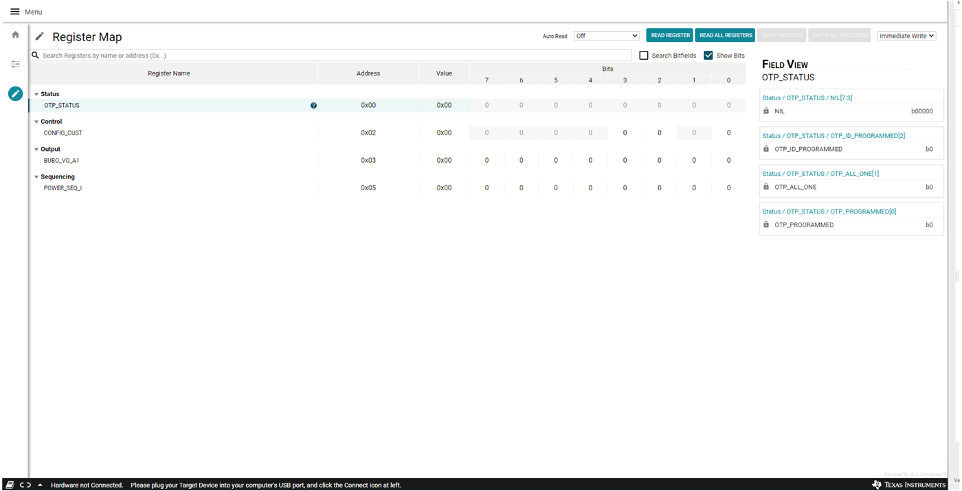
TPSM83102EVM GUI Register Map ScreenFigure 3-4 GUI Register Map Screen