SLVUD20 October 2024 DRV8376
2.4 Jumper Information
The DRV8376EVM has a few configurations that can be made with jumpers. Use these sections as a guide on how to make those configurations using jumpers.
Hall Sensors
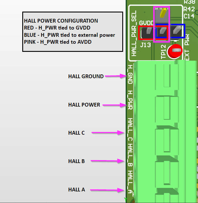 Figure 2-4 DRV8376EVM Hall
Configuration
Figure 2-4 DRV8376EVM Hall
ConfigurationThe connections that need to be made to the Hall terminal block are shown in Figure 2-4. The figure also shows how to configure the hall power. For externally supplied hall power, supply the power to TP12 and make sure there is a jumper where the blue rectangle is, as seen in the figure above.
VREF
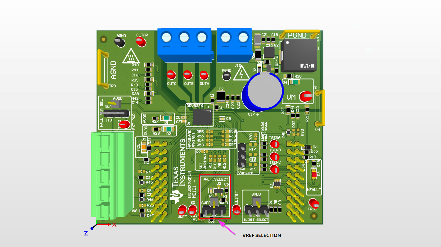 Figure 2-5 DRV8376EVM VREF Selection
Location
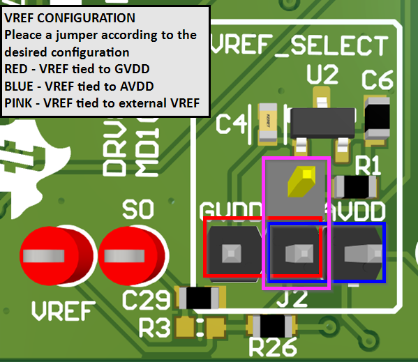 Figure 2-6 DRV8376EVM VREF
Configuration
Figure 2-6 DRV8376EVM VREF
ConfigurationILIMIT
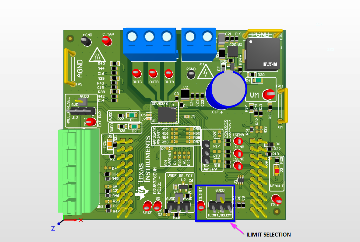 Figure 2-7 DRV8376EVM ILIMIT Selection
Location
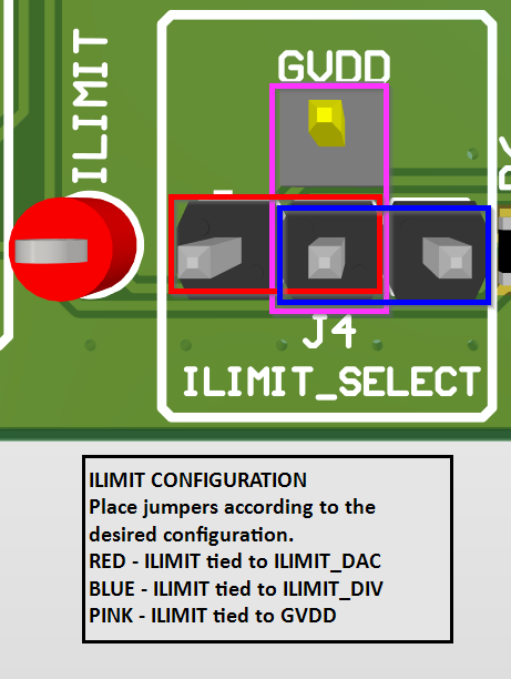 Figure 2-8 DRV8376EVM ILIMIT
Configuration
Figure 2-8 DRV8376EVM ILIMIT
ConfigurationLaunchXL-F280049C Connector Pins
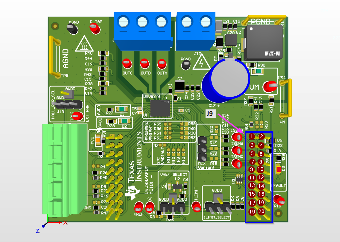 Figure 2-9 DRV8376EVM J9 Header
|
J9 Pin number (DRV8376EVM Schematic) |
DRV8376EVM Function |
LAUNCHXL-F280049C Function |
Description |
|---|---|---|---|
|
20 |
Not used |
3.3V |
3.3V LaunchPad supply |
|
19 |
Not used |
5V |
5V LaunchPad supply |
|
18 |
Not used |
PGA1/3/5_GND |
Not used |
|
17 |
AGND |
GND |
GND connection |
|
16 |
Not used |
GPIO13/SCIBRX |
Not used |
|
15 |
VSENVM |
ADCINA5 |
VM Bus voltage sense |
|
14 |
Not used |
GPIO40/SCIBTX |
Not used (HALLC internal use only) |
|
13 |
VSENC |
ADCINB0 |
Phase C voltage sense |
|
12 |
nSLEEP |
NC |
For internal use only |
|
11 |
VSENB |
ADCINC2 |
Phase B voltage sense |
|
10 |
Not used |
ADCINB3/VDAC |
Not used |
|
9 |
VSENA |
ADCINB1 |
Phase A Voltage Sense |
|
8 |
SCLK |
SPIACLK |
SPI clock (DRV8376 SPI Variant only) |
|
7 |
ISENA |
ADCINB2 |
Phase A current sense |
|
6 |
nFAULT (DNP) |
ADCINC4 |
For internal use only |
|
5 |
ISENB |
ADCINC0 |
Phase B current sense |
|
4 |
nSLEEP |
GPIO37 |
Active-low output sleep pin |
|
3 |
ISENC |
ADCINA9 |
Phase C current sense |
|
2 |
nFAULT |
GPIO35 |
Active-low input fault pin |
|
1 |
C_TAP/ILIM_DAC (populate only R32 or R33, not both) |
ADCINA1/DACB_OUT |
ADC for center tap sensing or DAC for ILIM voltage reference |
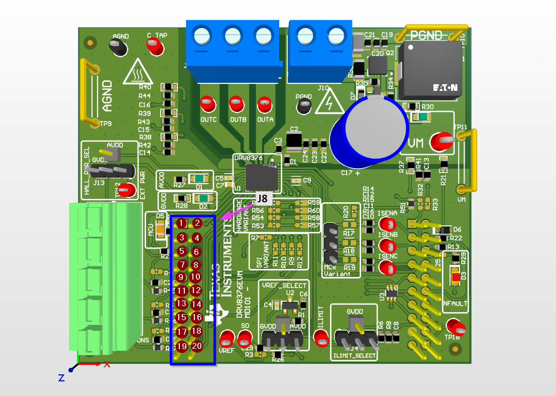 Figure 2-10 DRV8376EVM J8 Header
|
J8 Pin Number (DRV8376EVM Schematic) |
DRV8376EVM Function |
LAUNCHXL-F280049C Function |
Description |
|---|---|---|---|
|
20 |
INHA/HPA |
GPIO10/PWM6A |
PWM used to switch Phase A highside FET |
|
19 |
AGND |
GND |
GND connection |
|
18 |
INLA/HNA |
GPIO11/PWM6B |
PWM used to switch Phase A lowside FET |
|
17 |
nSCS |
SPIASTE |
SPI active-low chip select (DRV8316R only) |
|
16 |
INHB/HPB |
GPIO8/PWM5A |
PWM used to switch Phase B highside FET |
|
15 |
Not used |
NC |
Not used |
|
14 |
INLB/HNB |
GPIO9/PWM5B |
PWM used to switch Phase B lowside FET |
|
13 |
Not used |
NC |
Not used |
|
12 |
INHC/HPC |
GPIO4/PWM3A |
PWM used to switch Phase C highside FET |
|
11 |
Not used |
XRSn |
Not used |
|
10 |
INLC/HNC |
GPIO5/PWM3B |
PWM used to switch Phase C lowside FET |
|
9 |
SDI |
SPIAPICO |
SPI data input (DRV8376 SPI Variant only) |
|
8 |
HALLA |
GPIO58 |
HALL sensor A from motor |
|
7 |
SDO |
SPIAPOCI |
SPI data output (DRV8376 SPI Variant only) |
|
6 |
HALLB |
GPIO30 |
HALL sensor B from motor |
|
5 |
DRVOFF |
GPIO39 |
Active-high output to disable gate drivers |
|
4 |
HALLC |
GPIO18*/XCLKOUT |
HALL sensor C from motor |
|
3 |
Not used |
GPIO23/LED4 |
LED reserved on LaunchPad |
|
2 |
VREF |
GPIO25 |
For internal use only |
|
1 |
MCU_LED |
GPIO59 |
Visual feedback for LaunchPad connection |