-
TSW14J56 JESD204B High-Speed Data Capture and Pattern Generator Card
TSW14J56 JESD204B High-Speed Data Capture and Pattern Generator Card
TSW14J56 JESD204B High-Speed Data Capture and Pattern Generator Card User's Guide
The TI TSW14J56 evaluation module (EVM) is a next generation pattern generator and data capture card used to evaluate performances of the new TI JESD204B device family of high-speed analog-to-digital converters (ADC) and digital-to-analog converters (DAC). For an ADC, by capturing the sampled data over a JESD204B interface when using a high-quality, low-jitter clock, and a high-quality input frequency, the TSW14J56 can be used to demonstrate datasheet performance specifications. Using Altera JESD204B IP cores, the TSW14J56 can be dynamically configurable to support lane speeds from 600 Mbps to 12.5 Gbps, from 1 to 8 lanes, 1 to 16 converters, and 1 to 4 octets per frame with one firmware build. Together with the accompanying High-Speed Data Converter Pro Graphic User Interface (GUI), it is a complete system that captures and evaluates data samples from ADC EVMs and generates and sends desired test patterns to DAC EVMs.
Trademarks
Windows is a trademark of Microsoft Corporation.
1 Functionality
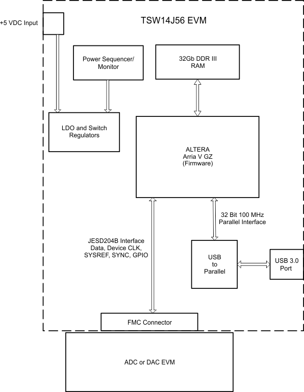
The TSW14J56EVM has a single industry standard FMC connector that interfaces directly with TI JESD204B ADC and DAC EVM's. When used with an ADC EVM, high-speed serial data is captured, de-serialized and formatted by an Altera Arria V GZ FPGA. The data is then stored into an external DDR3 memory bank, enabling the TSW14J56 to store up to 2G 16-bit data samples. To acquire data on a host PC, the FPGA reads the data from memory and transmits it on a high speed 32 bit parallel interface. An onboard high-speed USB 3.0 to parallel converter bridges the FPGA interface to the host PC and GUI.
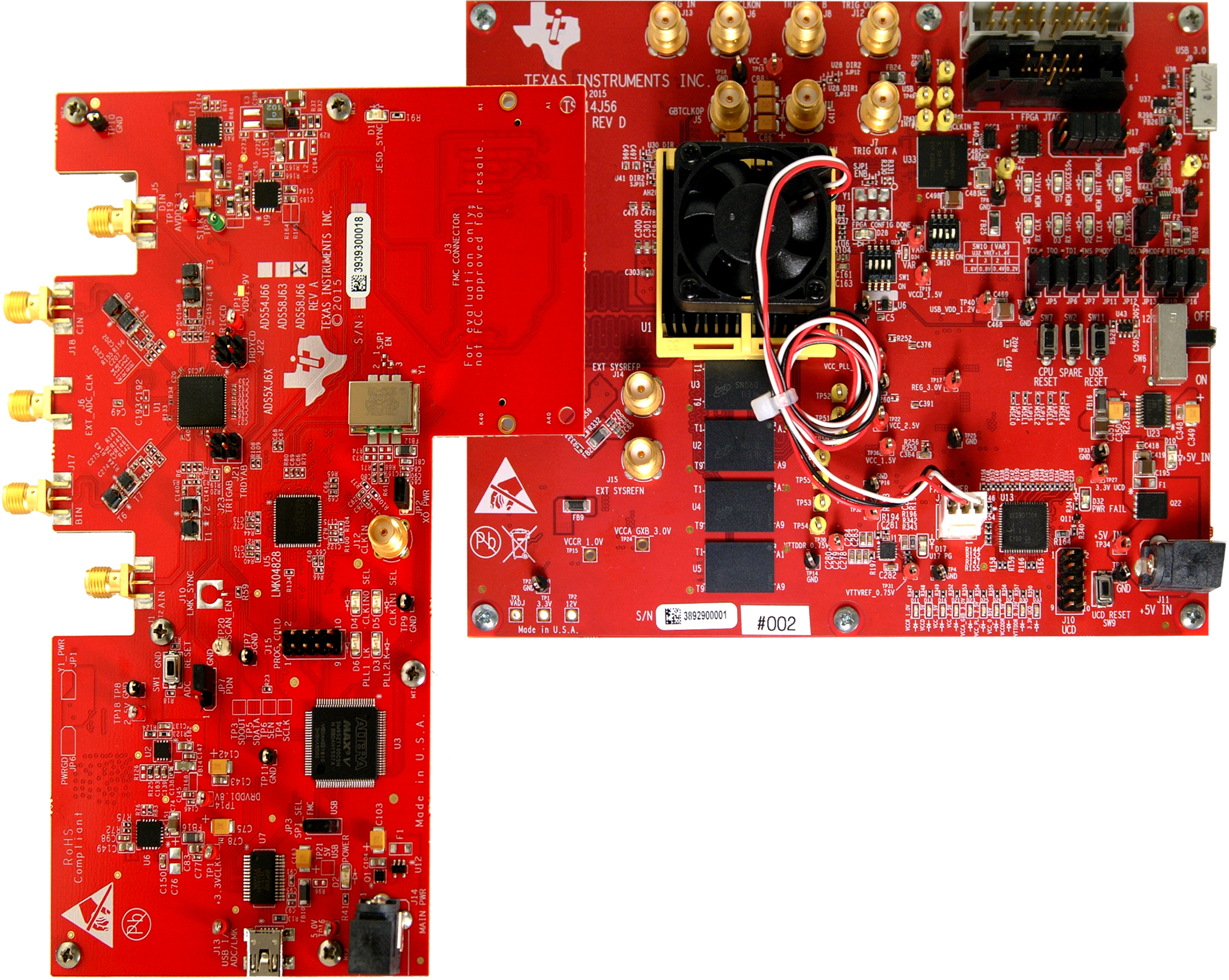
In pattern generator mode, the TSW14J56 generates desired test patterns for DAC EVMs under test. These patterns are sent from the host PC over the USB interface to the TSW14J56. The FPGA stores the data received into the board DDR3 memory module. The data from memory is then read by the FPGA and transmitted to a DAC EVM across the JESD204B interface connector. The board contains a 100-MHz oscillator used to generate the DDR3 reference clock and a option for a 10-MHz oscillator for general purpose use. Figure 1 shows the TI ADS58J63EVM plugged into the TSW14J56EVM.
The major features of the TSW14J56 are:
- Subclasses: 0 (backward compatible), 1, 2
- Support for deterministic latency
- Serial lanes speeds up to 12.5 Gbps
- 10 routed transceiver channels
- 32 Gb DDR3 SDRAM (split into four independent 512×164 Gb SDRAMs, total of 512M samples each). Quarter rate DDR3 controllers supporting up to 800-MHz operation
- 256K 16-bit samples of internal FPGA memory
- Supports 1.8, 2.5 and 3-V adjustable CMOS IO standard
- Option for general purposed 10 MH oscillator
- Onboard UCD90120A for power sequencing and monitoring
- Onboard Cypress CYUSB301X USB 3.0 device for JTAG and parallel interface to the FPGA
- Reference clocking for transceivers available through FMC port or SMAs
- Supported by TI HSDC PRO software
- FPGA firmware developed with Quartus II 14.0 and QSYS
- JESD RX IP core with support for:
- USB and JTAG reconfigurable JESD core parameters: L, M, K, F, HD, S, and more
- ILA configuration data accessible through USB and JTAG
- Lane alignment and character replacement enabled or disabled through USB and JTAG
- JESD TX IP core with support for:
- USB and JTAG reconfigurable JESD core parameters: L, M, K, F, HD, S, and more
- ILA data configured through USB and JTAG
- Character replacement enabled or disabled through USB and JTAG
- Dynamically reconfigurable transceiver data rate. Operating range from 0.600 to 12.5 Gbps
- JESD RX IP core with support for:
Figure 2 shows a block diagram of the TSW14J56 EVM.
1.1 ADC EVM Data Capture
New TI high-speed ADCs and DACs now have high-speed serial data that meets the JESD204B standard. These devices are generally available on an EVM that connects directly to the TSW14J56EVM. The common connector between the EVMs and the TSW14J56EVM is a Samtec high-speed, high-density FMC connector (SEAF-40-05.0-S-10-2-A-K) suitable for high-speed differential pairs up to 21 Gbps. A common pinout for the connector across a family of EVMs has been established. At present, the interface between the EVMs and the TSW14J56EVM has defined connections for 10 lanes of serial differential data, two device clock pairs, two JESD204B SYSREF and SYNC pairs. There are four over-range single-ended indicators, 12 spare general purpose CMOS I/O pins, and 29 spare differential LVDS or 58 single-ended CMOS signals. The board has a spare SMA interface to the FPGA, 4 spare dip switches, a pushbutton switch, several spare test points routed to the FPGA and 8 status LED's.
The data format for JESD204B ADCs and DACs is a serialized format, where individual bits of the data are presented on the serial pairs commonly referred to as lanes. Devices designed around the JESD204B spec can have up to 8 lanes for transmitting or receiving data. The firmware in the FPGA on the TSW14J56 is designed to accommodate any of TI's ADC or DAC operating with any number of lanes from 1 to 8.
The GUI loads the FPGA with the appropriate firmware and a specific JESD204B configuration, based on the ADC device selected in the device drop down window. Each ADC device that appears in this window has an initialization file (.ini) associated to it. This .ini file contains JESD information, such as number of lanes, number of converters, octets per frame, and other parameters. This information is loaded into the FPGA registers after the user clicks on the capture button. After the parameters are loaded, synchronization is established between the data converter and FPGA and valid data is then captured into the on-board memory. See the High-Speed Data Capture Pro GUI Software User's Guide SLWU087 and section 2.3 in the guide for more information. Several .ini files are available to allow the user to load pre-determined ADC JESD204B interfaces. For example, if the user selects the ADC called "ADS42JB69_LMF_421", the FPGA will be configured to capture data from the ADS42JB69EVM with the ADC JESD interface configured for 4 lanes, 2 converters, and 1 octet per frame.
The TSW14J56 device can capture up to 2G 16-bit samples at a maximum line rate of 12.5 Gbps that are stored inside the on-board DDR3 memory. To acquire data on a host PC, the FPGA reads the data from memory and transmits parallel data to the on-board high-speed parallel-to-USB converter.
1.2 DAC EVM Pattern Generator
In pattern generator mode, the TSW14J56EVM generates desired test patterns for DAC EVMs under test. These patterns are sent from the host PC over the USB interface to the TSW14J56. The FPGA stores the data received into the on-board DDR3 memory. The data from the memory is then read by the FPGA, converted to JESD204B serial format, then transmitted to a DAC EVM. The TSW14J56 can generate patterns up to 2G 16-bit samples at a line rate up to 12.5 Gbps.
The GUI comes with several existing test patterns that can be download immediately. The GUI also has a pattern generation tool that allows the user to generate a custom pattern, then download it to the on-board memory. See the High-Speed Data Capture Pro Software User's Guide SLWU087 for more information. Like the ADC capture mode, the DAC pattern generator mode uses .ini files to load predetermined JESD204B interface information to the FPGA.

