-
Clocking for Medical Ultrasound Systems
Clocking for Medical Ultrasound Systems
Trademarks
All other trademarks are the property of their respective owners.
1 Introduction
Medical ultrasound systems use sound waves to generate images of the body. They do this by transmitting an ultrasound wave into the body and then receiving the echo. This echo is processed to generate an image.
This transmission and reception of the ultrasound signals has to be highly synchronized to achieve the best results. Precision Clocking is crucial to ensure that the information displayed has minimum artifacts.
Phase noise (frequency domain) or Jitter (time domain) is a measure of how much a clock signal’s phase or switching edge deviates from its ideal position and is an important parameter that can determine the impact of reference clocks on the ultrasound image. For example, ultrasound often uses the Doppler Effect to determine the direction and magnitude of blood flow. Higher phase noise can lead to artifacts occurring in Doppler images such as speckles which represent errors in the calculation and display of blood flow. In Doppler imaging, the strong reflection from close surfaces and weak signals from higher depths results in a high dynamic range and jitter on the reference clock can potentially create undesired artifacts.
TI’s popular high-performance AFEs need a jitter performance of less than 400 fs to perform optimally especially in the CW Doppler mode. Another important consideration for Doppler imaging is the phase noise at low-offset frequency (typically 1 kHz) to resolve between objects which are very close to each other.
Figure 1-1 is a representative high-level block diagram.
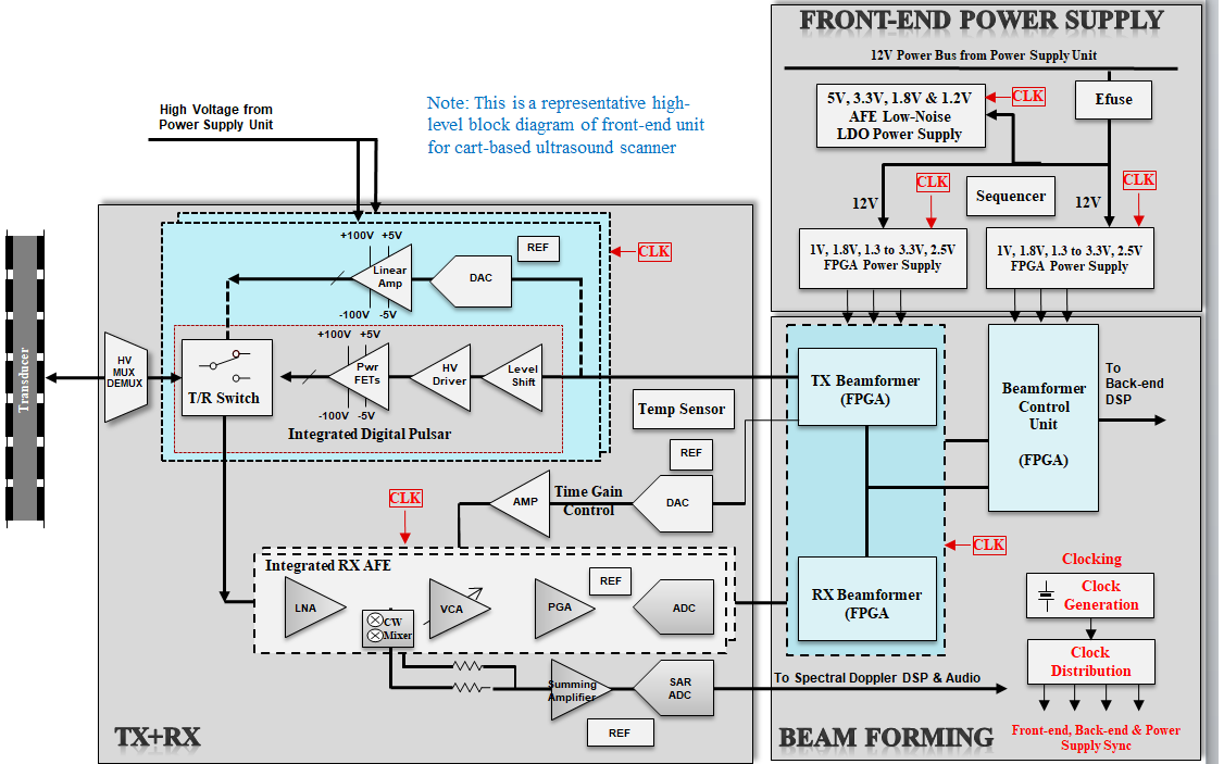 Figure 1-1 Representative Block
Diagram (Front-end Unit).
 There are various subsystems in the ultrasound systems which need clocking:
- Front End:
- Transmit Pulsers – Need several copies of very low jitter, high frequency clocks in the range of 200 MHz to achieve good beam focusing. (An example of ultra-low jitter reference source from TI is the LMK61E2 family of crystal oscillators which also has a very good close-in phase noise of –140 dBc/Hz at 1-kHz offset for a 200-MHz carrier. Examples of ultra-low additive jitter buffers from TI that can be used to distribute low noise reference clocks are LMK1C110x for LVCMOS, LMK0030X for differential outputs.)
- Receive AFEs – The most sensitive component of the receive AFE is the ADC clock. This clock needs to be very low jitter and have low phase noise at 1-kHz offset. Additionally for beam-forming, several low skew copies of highly synchronized clocks for all the AFEs to ensure that the data is sampled simultaneously. Frequencies are in the range of 40 to 125 MHz. (An example of a low skew distribution buffer family from TI is LMK0030X.)
- CW Doppler – Requires two clocks namely 16 × fCW and 1 × fCW. 16 × fCW is used to generate LO signals with 16 accurate phases internal to the AFE whereas the 1 × fCW is used for synchronization of multiple AFE devices. Very good phase noise performance is crucial to determine the frequency shift and this specification is applicable only for the 16× clock as the 1× clock is used primarily for synchronization. The range for the 16× clock is typically from 16 to 128 MHz. (An example of a high performance dual-loop jitter attenuator/clock generator device family from TI suitable for generating CW Doppler clocks is LMK04832.
- Beam-forming – For transmit and receive beam-forming the clocks need to be highly synchronized (LMK0030x fanout buffers). Transmit beam-forming focuses the ultrasound wave-front. Precise timing is required and any variation in the clock edges (jitter) can lead to loss of focus. The loss of precise synchronization between transmit and receive beamforming can also result in loss of image resolution.
- Clock distribution FPGAs – FPGAs can also be used to generate the clocks needed for
transmit and receive timing, but the jitter performance of these clocks
is typically not nearly as good as specialized clocking ICs. The jitter
then needs to be cleaned by external jitter cleaners. (An example of
high-performance, dual-loop jitter attenuator from TI is the
LMK04832.)
Another important recent development is the introduction of JESD204B ADC (ADS52J90) and AFEs (AFE58JD28, AFE58JD48) which provide higher data converter resolution and front-end sensitivity by synchronizing multiple devices. This synchronizing scheme requires very precise clocking as defined in JESD204B; TI’s LMK04832 supports JESD204B clocking enabling the highest system level performance.
- Power Supply:
- All the power supplies within the ultrasound system are often synchronized to one master clock to avoid the effects of switching noise appearing as artifacts in the image (through filtering). These power supplies typically operate in the range of 100 kHz to 1 MHz. Higher switching frequencies often result in smaller magnetic components but also operate closer to the dynamic range of the ultrasound signals themselves. Synchronizing all switching power supplies to the same (lower) frequency and then filtering at that frequency can avoid any coupling of this noise into the ultrasound signal chain. In addition, spread spectrum clocking can help to reduce EMI effects. (Examples of flexible clock generators with spread-spectrum generation capability used to minimize EMI in the system includes CDCE913 and CDCE6214.)
- Backend:
- Once the signals are digitized and provided to the digital post-processing sub-systems, the jitter is then not as critical. However it is desirable to have clean clocks throughout the entire system – to ensure maximum performance and lower overall noise in the system.
- FPGAs for image processing require frequencies which include the sampling frequency and others needed for communication and internal logic blocks. CDCM6208, LMK033x8, CDCE6214, and LMK60E2 are some of the TI devices which can be used to generate the relevant frequencies.
- DSPs and Processors for image processing require common frequencies like 100 MHz. (CDCM6208, LMK03328, CDCE6214)
- External communication – PCI, PCI Express, USB,
Ethernet, and so forth, that typically require
24-, 48-, and 100-MHz clocks along with buffers to distribute them to the various peripherals. TI clock generators such as CDCM6208, CDCE6214, and clock buffers LMK00334, LMK00338, are PCIe Gen1 to Gen5 compliant and meet the system requirements.
System designers prefer using clocks with the features listed as follows:
- Programmability and scalability – provides flexibility in the frequency floor-plan to ensure optimum system performance along with supporting additional features or variations at a later date – without change in hardware. (LMK61E2 reference oscillator, any LMK or CDC clock generator)
- JESD204B support (gaining traction in next-generation high-performance AFEs, for example, the LMK04832)
- High integration with fewer parts and smaller board solution size (LMK04832, LMK00328, CDCE9XX and so on.)
- Low-power dissipation (CDCE6214)
- Fully-differential clocking wherever possible in the signal chain (common-mode noise rejection).
Precision clocking can be achieved by having ultra-low noise clock sources, generators/dividers, distributors and buffers. The clocks generators are accurate and typically have lower phase noise when integer mode PLL and output dividers are used versus fractional mode PLL and/or fractional output dividers – that could introduce additional phase noise and potentially some small frequency synthesis error.
The impact can be minimized by ensuring that the front-end signal chain uses integer dividers exclusively to generate the clocks needed for the performance-critical front-end clock.
For the fanout of clock signals it is important to select buffers with very low additive jitter, otherwise the noise floor of a high-quality source clock (that is, LMK61E2) would degrade significantly each time it is buffered. Suitable buffers for this kind of application are the LMK0030x family (differential) and the LMK1C110x family (LVCMOS), that have very low additive jitter and excellent noise-floor.
TI’s clock generator, dividers and low jitter buffers are some key components which help achieve this required performance.
Table 1-1 and the Figure 2-1 show a typical clock tree for an ultrasound system. This clock tree demonstrates the use of various reference clocks for different building blocks – Transmit, Receive, FPGAs, Processors, power supply, and so on.
|
Number of CLKS |
Frequency |
Format |
Target |
TI Device |
|---|---|---|---|---|
|
92 |
> 250 MHz |
LVCMOS |
TX (DAC + AMP clock) |
LMK04832+LMK0030X(1) |
|
12 |
Up to 320 MHz |
LVDS/LVPECL/LVCMOS |
TX (Beam-former clock) |
LMK04832+LMK0030X(1) |
|
2 |
120 MHz |
LVDS |
FPGA (AWG) |
LMK04832+LMK0030X |
|
2 |
200 MHz |
LVDS |
FPAG (Transmit) |
LMK04832+LMK0030X |
|
1 |
200 MHz |
LVDS |
FPGA (Receive) |
LMK03328+CDCLVD12XX |
|
16 |
100 kHz to 500 kHz |
LVCMOS |
Power Supply |
CDCE913+LMK1C110X |
|
12 |
Up to 128 MHz |
LVDS |
AFE (CW 16x clock) |
LMK04832+LMK0030X(1) |
|
12 |
Up to 125 MHz |
LVDS/LVPECL |
AFE (ADC sampling clock) |
LMK04832+LMK0030X(1) |
|
12 |
Up to 8 MHz |
LVDS |
AFE (CW 1x clock) |
FPGA |
|
1 |
122.88 MHz |
LVDS |
DSP |
LMK03328 |
|
3 |
100 MHz |
LVDS |
DSP |
LMK03328 |
|
1 |
24.576 MHz |
LVCMOS |
Audio Codec |
LMK03328 |
- Phase-noise performance critical clock.
| Value |
TI Device | |||||
|---|---|---|---|---|---|---|
| 80 MHz | 96 MHz | 100 MHz | 160 MHz | 200 MHz | 320 MHz | LMK61E2 |
2 Clock Tree
Example: Clock tree for 192-channel ultrasound cart-based system.
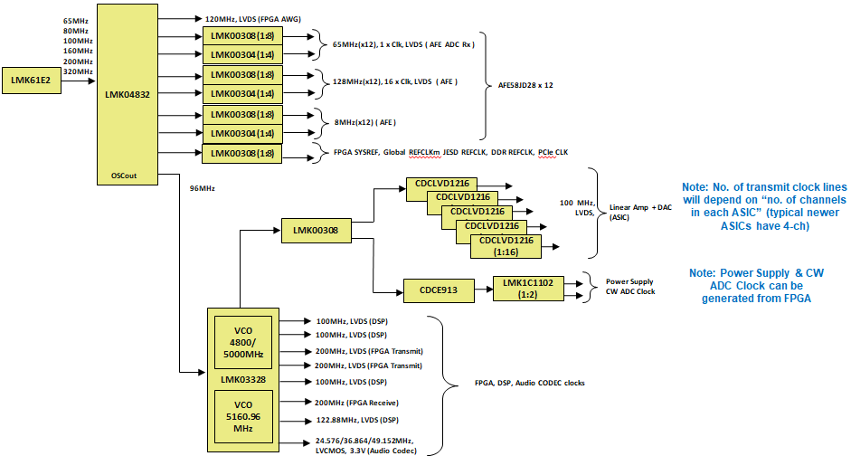 Figure 2-1 Front-End Unit and Back-End
Unit
Figure 2-1 Front-End Unit and Back-End
UnitTests were conducted to demonstrate the total additive jitter and also jitter in various clock configurations for the clock tree by using individual evaluation modules from the different clocking components.
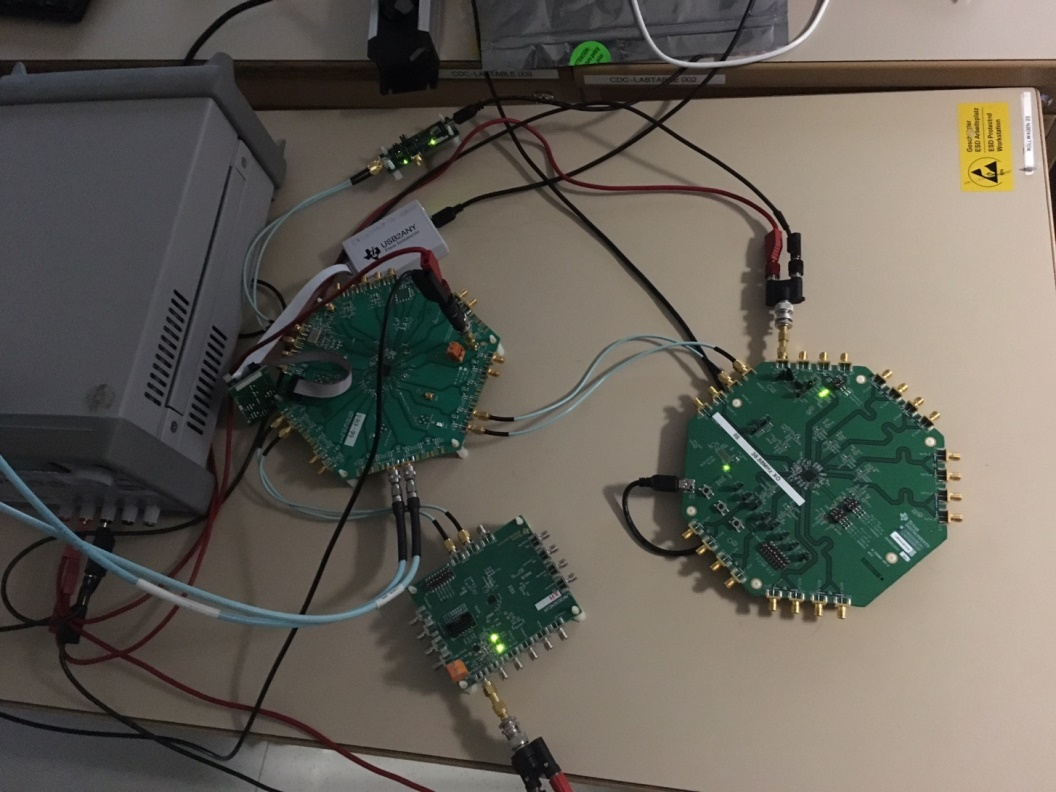 Figure 2-2 Different Clocking Components
The following graphs demonstrate the noise performance of the actual signals as measured on a signal source analyzer.
Demonstration 1:
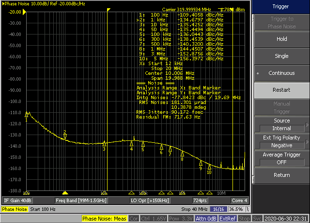
| Reference = 320 MHz LVPECL | ||||
| Integrated RMS Jitter (12 kHz-20 MHz) - 90 fs |
Demonstration 2:
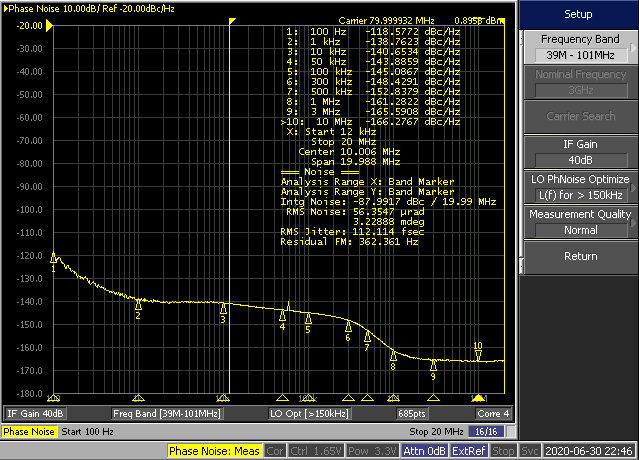
| Reference = 320 MHz from LMK61E2 and LMK04832 output = 80 MHz LVPECL | ||||
| Integrated RMS Jitter (12 kHz-20MHz) - 112 fs |
Demonstration 3:
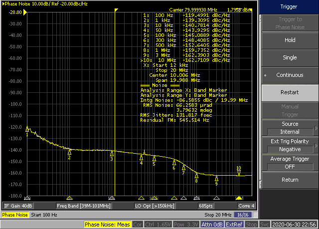
| Input = 80 MHz from LMK04832 and output = 80 MHz LVPECL | ||||
| Integrated RMS Jitter (12 kHz-20 MHz) - 132 fs |
A summary of the three demonstrations follows:
- The total integrated RMS jitter for the LMK61E2 and LMK04832 is 116 fs (RMS). The LMK0030X adds just 70 fs (RMS) to the output of LMK04832.
- The total integrated RMS jitter from LMK61E2 to the output of LMK0030X is just 132 fs.
This clock tree jitter is root-mean square added to the ADC aperture jitter and compared against the jitter requirement derived from the SNR of the ADC to make sure that the clock tree is not degrading ADC performance.
Since the total integrated RMS jitter of the clock tree presented here is low, therefore it will not limit the ADC performance in most ultrasound applications.
 Figure 2-6 Comparison of LMK61E2 to LMK0030X
Figure 2-7 illustrates the PN of various clock devices.
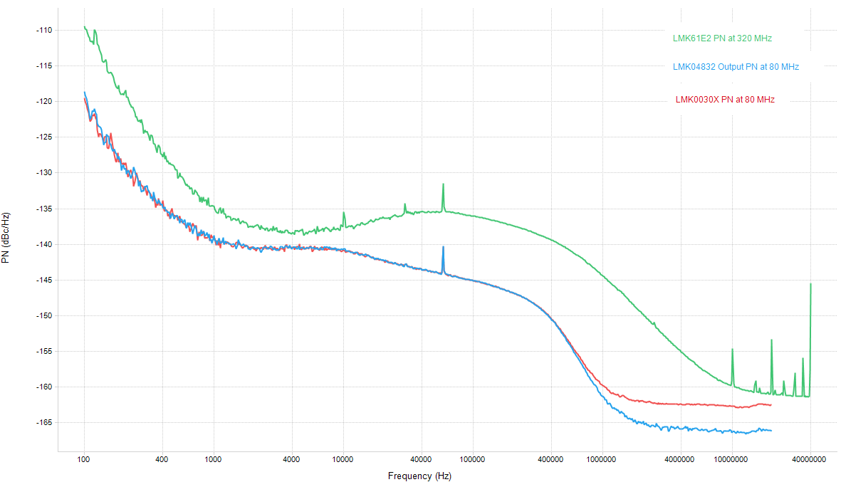 Figure 2-7 PN for Various Clock Devices Normalized to 1 GHz.
 3 Summary and Conclusion
The TI LMK series of Clock devices offer excellent additive jitter performance throughout the entire clock chain – which are ideally suited for ultrasound applications.
- The end-to-end jitter is well within the required limits of TI's high performance AFEs to achieve optimal performance. This low end-to-end jitter of TI’s clock devices ensures system designers get the maximum performance while also providing sufficient headroom for other factors like supply noise or coupling that might degrade the clock performance.
- For typical ultrasound applications it is possible to achieve low noise clocking by ensuring very low reference clock phase noise and edge jitter.
- With the introduction of JESD204B AFE (AFE58JDxx) and ADC (ADS52J90), the dual-loop jitter cleaner/clock generator LMK04832 is JESD204B-compliant and meets the stringent phase noise and jitter requirements of the new AFE/ADC parts with sufficient margin. The systems designed with the LMK04832 provide additional benefits such as:
- Low 1-kHz close-in phase noise
- Better VCO noise performance ensures lower noise floor
- Higher phase detector operating rates that further reduce PLL noise
- Integrated LDOs
4 Revision History
Changes from Revision * (September 2017) to Revision A (September 2020)
- Updated most of the application report for revision A.Go