SNAA361A april 2022 – may 2023 LMX2820
4.2 Active Loop Filter Implementation
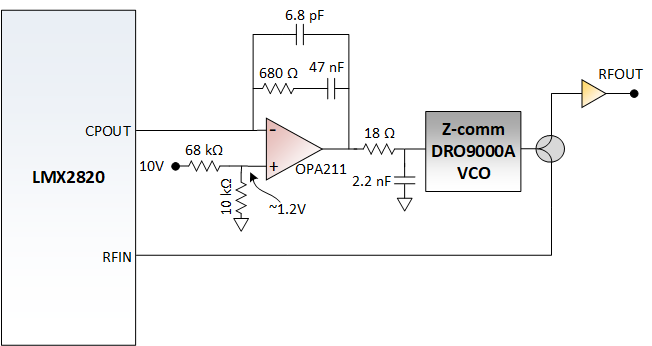
Figure 4-4 shows the block diagram for the external VCO and the active loop filter. There are a few key elements to highlight with the topology. When using the external VCO, there is no internal feedback mechanism to feed the PFD circuit. Use an external splitter to split the VCO output to the LMX2820 RF input and to the ultimate synthesizer output. If needed, use an external RF amplifier to boost the synthesizer output and compensate for the splitter loss.
The op amp is a critical component. Select a device that is low noise and supports rail-to-rail outputs. If the output cannot get down to 0 V, then utilizing the entire tuning range is not possible. For a single supply operation, bias the positive terminal at a suitable common-mode voltage. This voltage is roughly half of the maximum charge pump voltage from the device. For this design, a voltage divider operating on a 10-V rail sets the Vcm to 1.2 V.
The op amp is the OPA211. This device has a very low output noise voltage with suitable bandwidth and rail-to-rail output capability. Table 4-3 shows the key specs of the OPA211A.
| Parameter | Specification |
|---|---|
|
Low Voltage Noise (1 kHz) |
1.1 nV/√Hz) |
|
Gain BW Product (G = 100) |
80 MHz |
|
Slew rate |
27 V/μs |
 Figure 4-4 Block Diagram of the External
VCO Configuration