SNAA361A april 2022 – may 2023 LMX2820
4.3 External VCO Performance Results
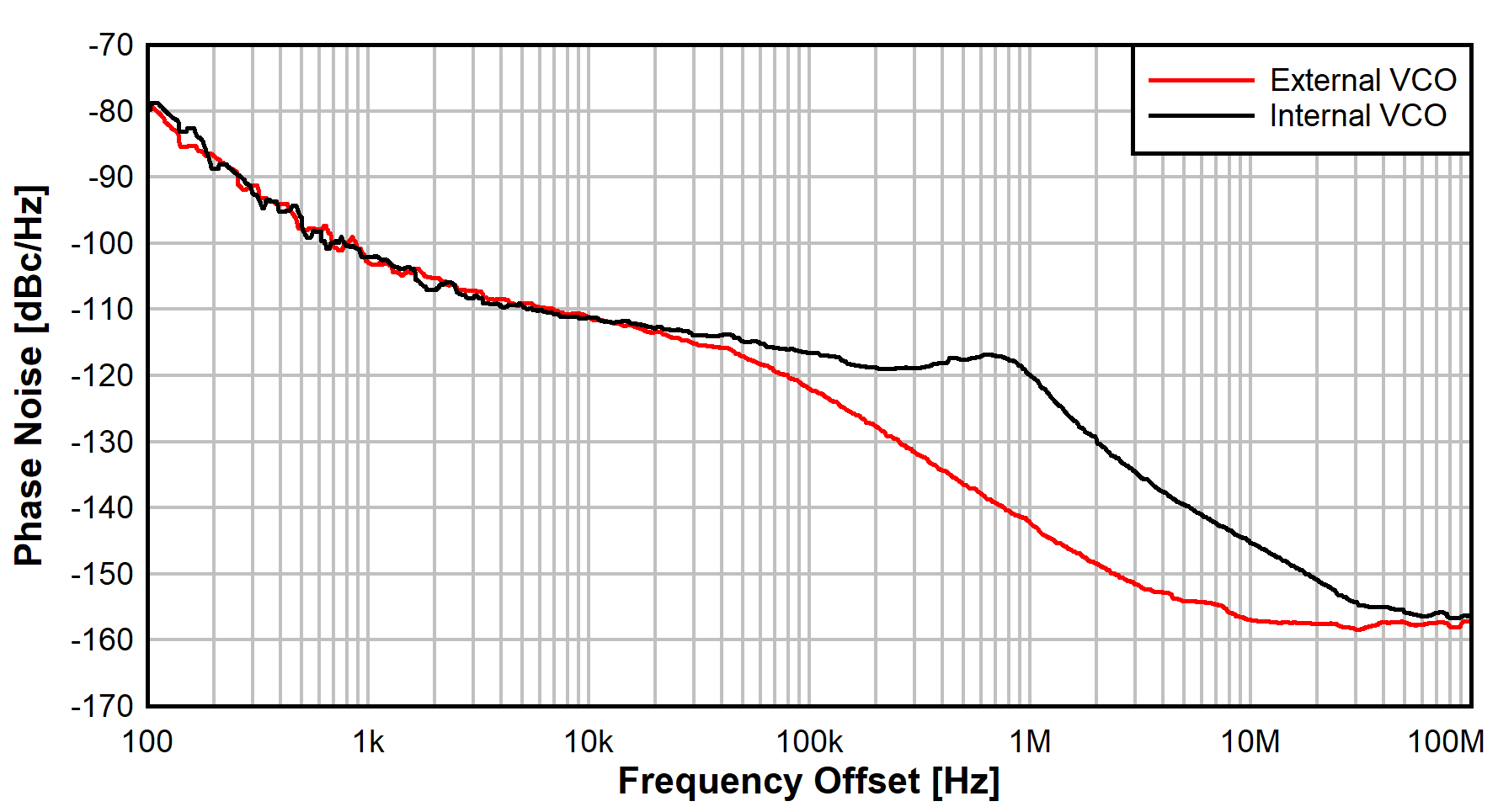
Figure 4-5 shows the external VCO phase noise plot compared to the LMX2820 operating with internal VCO. The SMA100B signal generator provides the reference signal. Reference signal power from the generator is set to 14 dBm to compensate for board trace losses and to ensure a large signal swing (and hence high slew rate) at the reference pin input of the LMX2820. The performance includes active loop filter with the OP211A op amp and the Qorvo NBB-312-T1 output power amplifier. Table 4-4 lists the RMS jitter performance at 9 GHz integrated from 10 kHz to 40 MHz. The phase noise plot shows equivalent performance between the internal VCO and the external VCO out to around a 10-kHz offset. Performance less than 10-kHz offset is still dominated by PLL and reference frequency performance. After which, the superior performance of the external VCO itself dominates. As an example, the spot noise improvement at 1-MHz offset between the external VCO and internal VCO is over 20 dB. Overall, the external VCO with active loop filter yields over a 20-fs improvement in RMS jitter.
 Figure 4-5 External VCO Phase Noise
Compared to LMX2820 Internal VCO
Figure 4-5 External VCO Phase Noise
Compared to LMX2820 Internal VCO| PFD | N-Divider | RF Out | Internal VCO | External VCO |
|---|---|---|---|---|
|
375 MHz |
24 |
9000 MHz |
37.9 fs |
13.2 fs |