SNAU263A February 2022 – July 2022
- Abstract
- Trademarks
- 1Introduction
- 2EVM Quick Start
- 3EVM Configuration
-
4EVM Schematics
- 4.1 Power Supply Schematic
- 4.2 Alternative Power Supply Schematic
- 4.3 Power Distribution Schematic
- 4.4 LMK5B33216 and Input Reference Inputs IN0 to IN1 Schematic
- 4.5 Clock Outputs OUT0 to OUT3 Schematic
- 4.6 Clock Outputs OUT4 to OUT9 Schematic
- 4.7 Clock Outputs OUT10 to OUT15 Schematic
- 4.8 XO Schematic
- 4.9 Logic I/O Interfaces Schematic
- 4.10 USB2ANY Schematic
- 5EVM Bill of Materials
- 6Appendix A - TICS Pro LMK5B33216 Software
- 7Revision History
3.10 Typical Phase Noise Characteristics
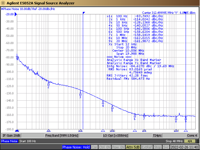
These plots show the typical phase noise performance for common frequencies outputted from the BAW (VCO3).
The EVM configuration used to obtain these measurements is as follows:
- XO frequency = 48 MHz (Onboard TCXO)
- Outputs were configured as HSDS outputs following the methods described in Section 3.9.
 Figure 3-12 APLL3 312.5-MHz Phase Noise Performance.
  Figure 3-14 APLL3 125-MHz Phase Noise Performance.
  Figure 3-13 APLL3 156.25-MHz Phase Noise Performance.
  Figure 3-15 APLL3 100-MHz Phase Noise Performance.