SNAU274 December 2021
5 Schematics
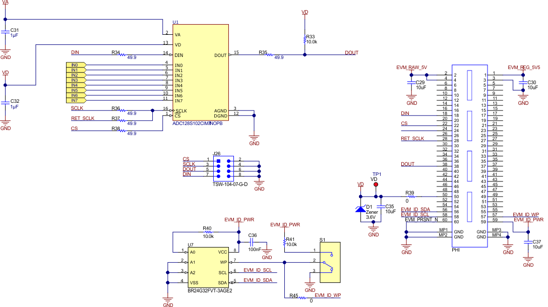
Figure 5-1 through Figure 5-3 illustrate the schematics for the ADC128S102EVM.
 Figure 5-1 ADC128S102EVM Schematic Page
1: Analog Inputs
 Figure 5-2 ADC128S102EVM Schematic Page
2: ADC and Digital Communications
 Figure 5-3 ADC128S102EVM Schematic Page
3: Power Tree