SNAU288
December 2023
LMX1906-SP
1
Description
Features
Applications
5
1
Evaluation Module Overview
1.1
Introduction
1.2
Kit Contents
1.3
Specification
1.4
Device Information
2
Hardware
2.1
Setup
2.1.1
Evaluation Setup Requirement
2.1.2
Connection Diagram
2.1.2.1
How to Enable Full SPI Control
2.1.3
Power Requirements
2.1.4
Pin Mode Strapping
2.1.5
Reference Clock
2.1.5.1
Output Connections
2.1.5.2
Header Information
2.1.5.3
Default Configuration
2.1.5.4
How to Generate SYSREF
2.1.5.5
Multiplier Mode Example
2.1.5.6
Divider Mode Example
2.1.5.7
Hybrid Mode: SPI and Pin Mode
3
Software
3.1
Software Installation
3.2
Software Description
3.3
USB2ANY Interface
4
Implementation Results
4.1
Buffer, Divider, and Multiplier Modes
4.2
SYSREF Generation
4.3
SYSREF Delay Generators
5
Hardware Design Files
5.1
Schematic
5.2
PCB Layout
5.2.1
PCB Layer Stack-Up
5.3
Bill of Materials
6
Additional Information
6.1
Troubleshooting Guide
6.1.1
General Guidance
6.1.2
If Output Is Not Seen on CLKOUT
6.1.3
If Device Features Are Not Active
6.1.4
If Multiplier Frequency Is Not Accurate
6.1.5
If Divider Frequency Is Not Accurate
6.1.6
If SYSREF Is Not Observed
6.2
Trademarks
5.1
Schematic
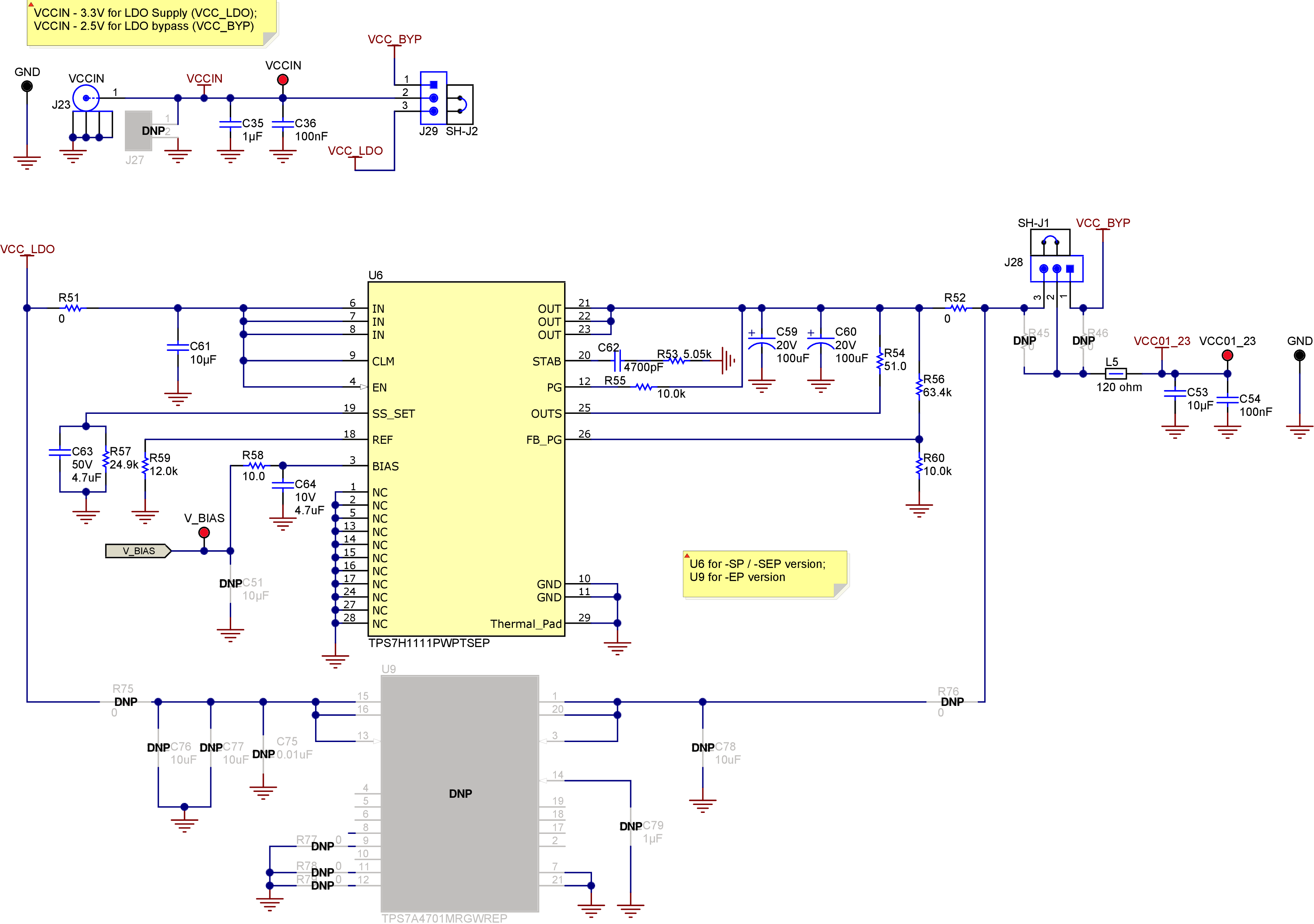
Figure 5-1
Power Supply
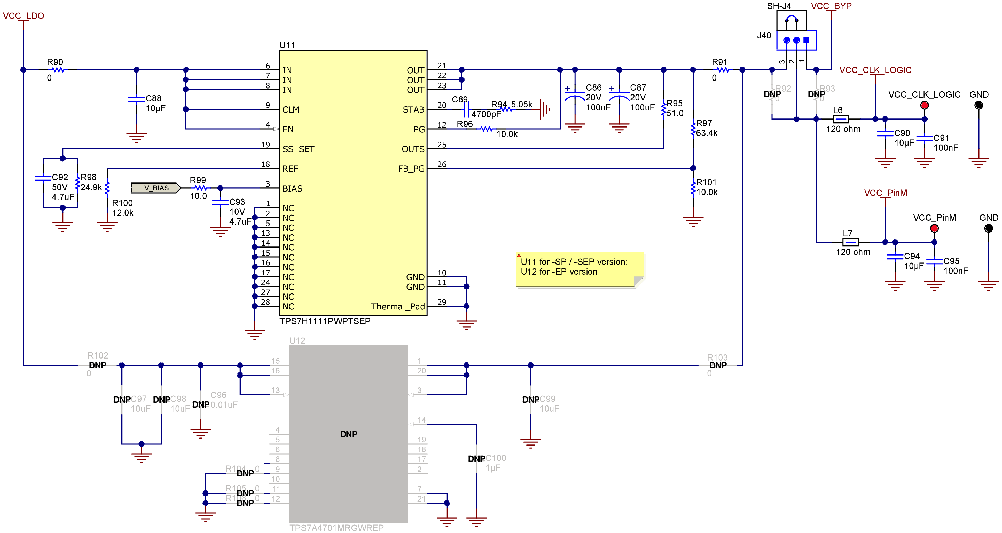
Figure 5-2
Power Supply
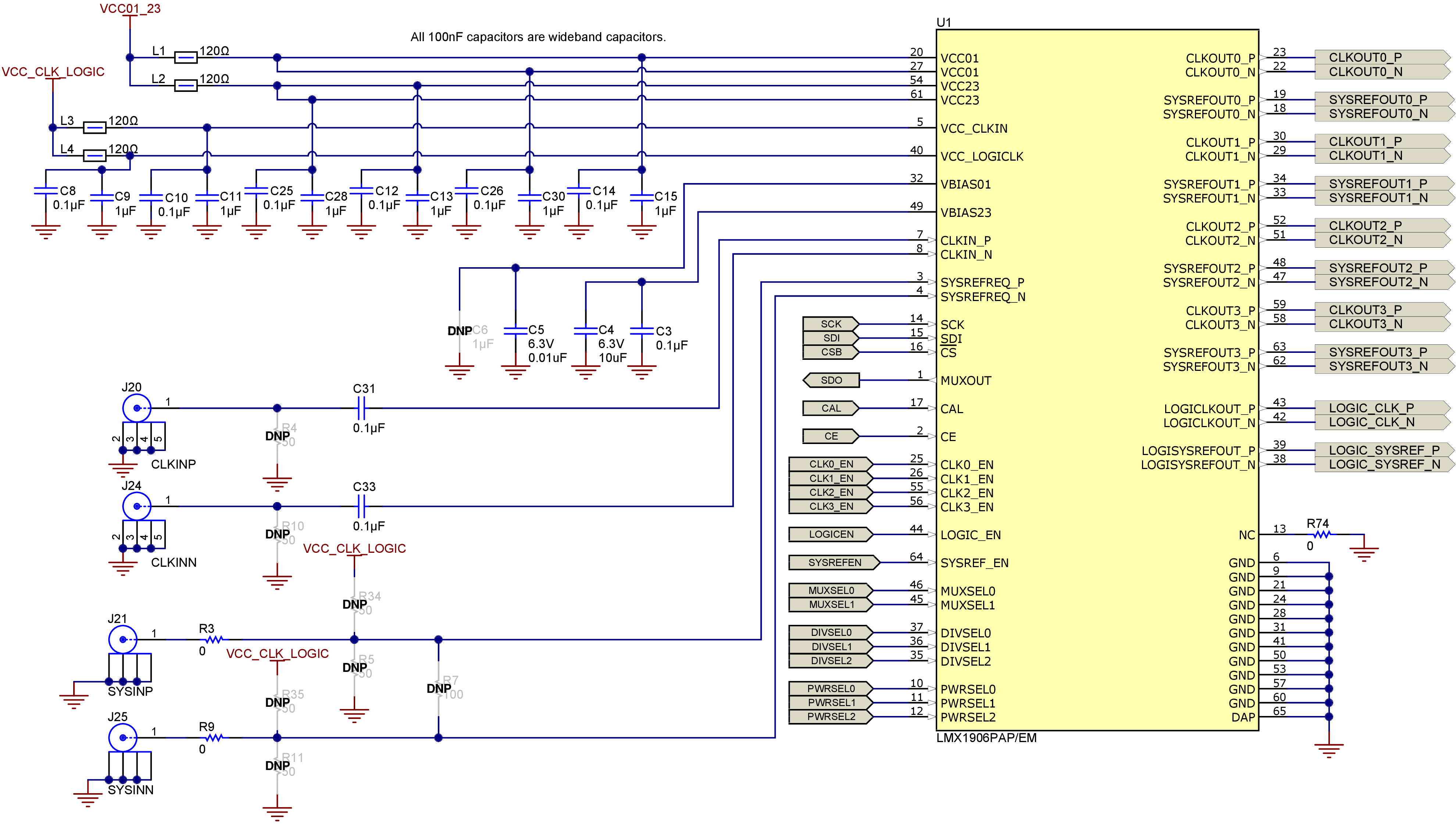
Figure 5-3
LMX1906-SP
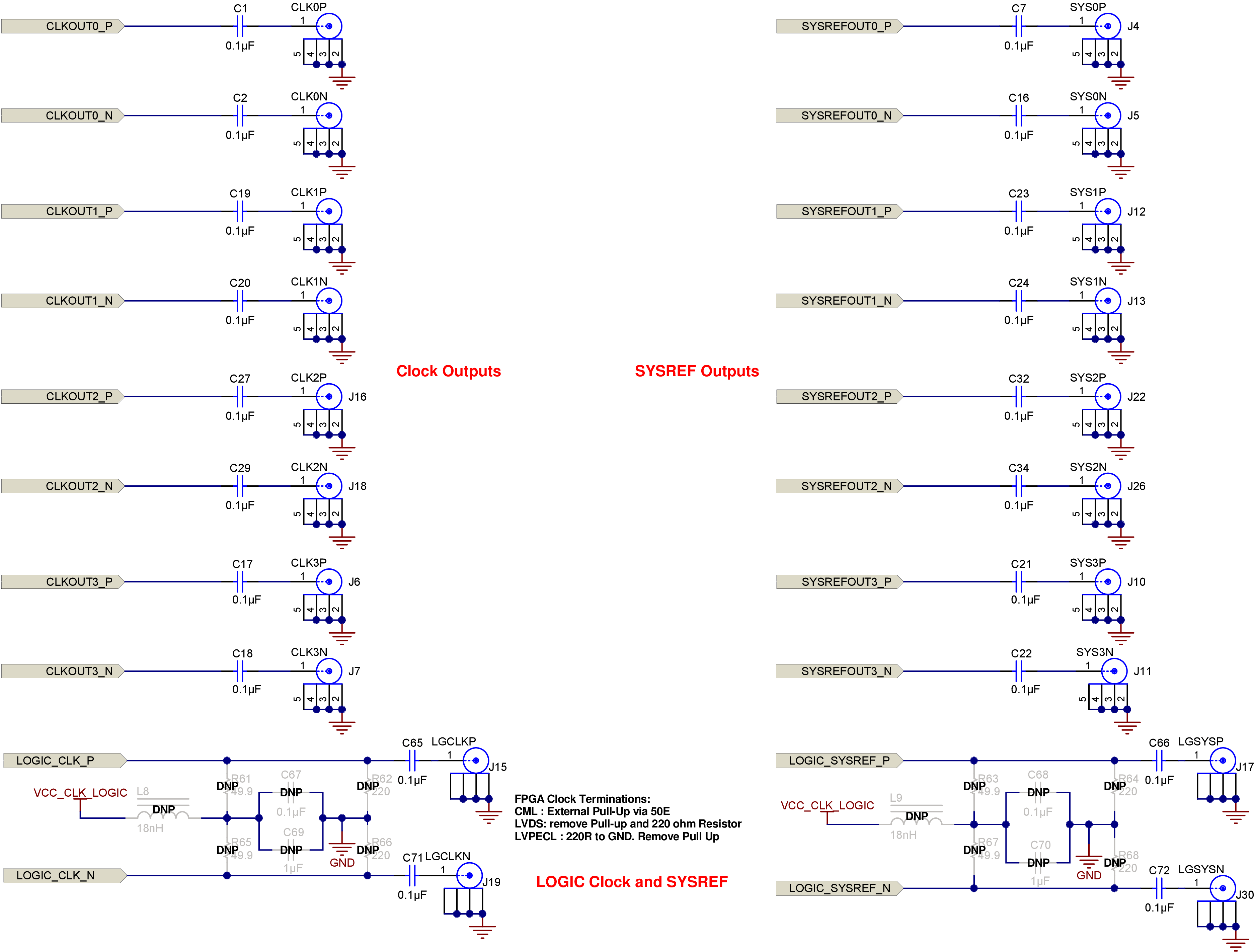
Figure 5-4
Clock Input, Clock Output Interface
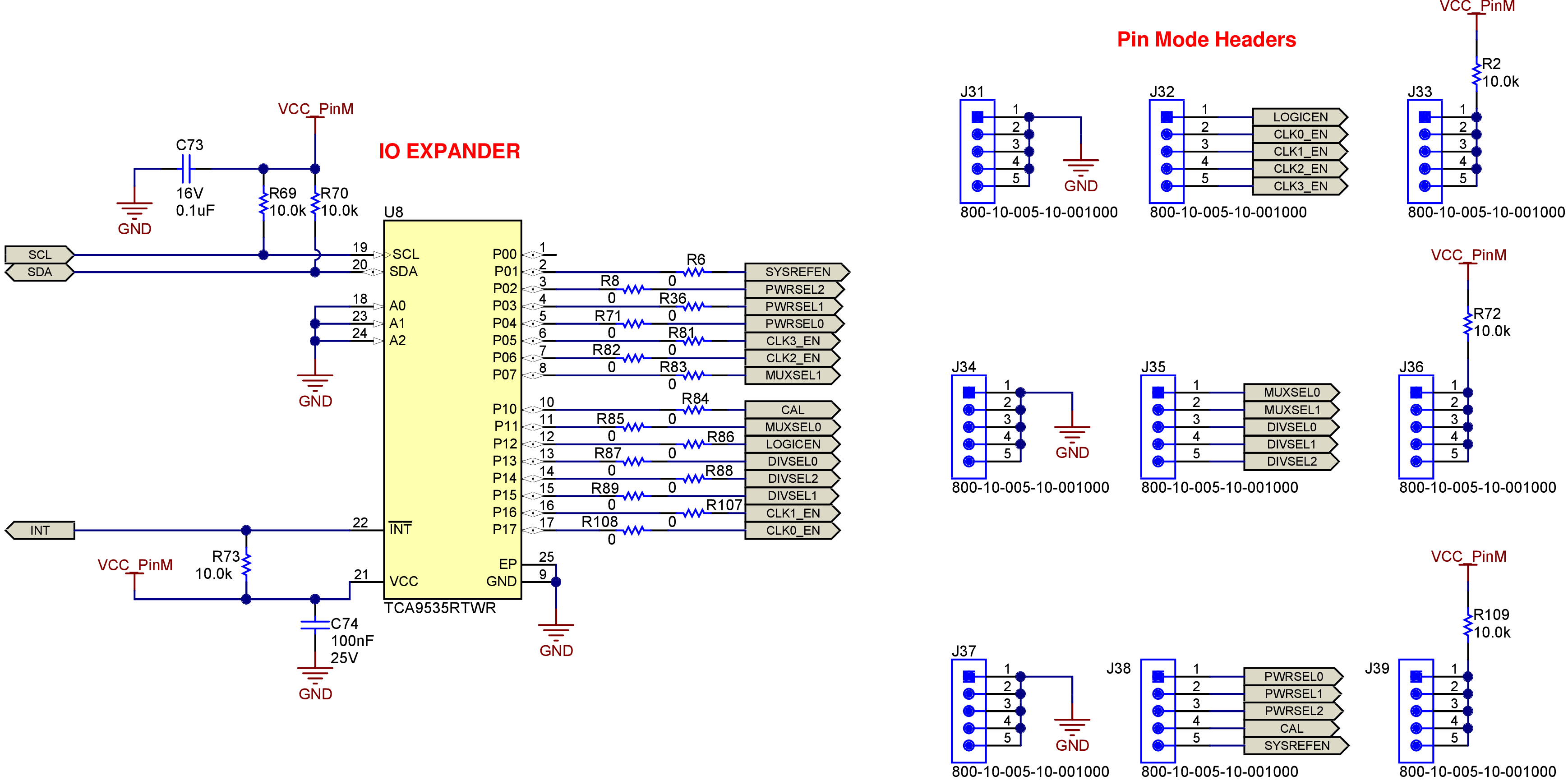
Figure 5-5
IO Interface
Figure 5-6
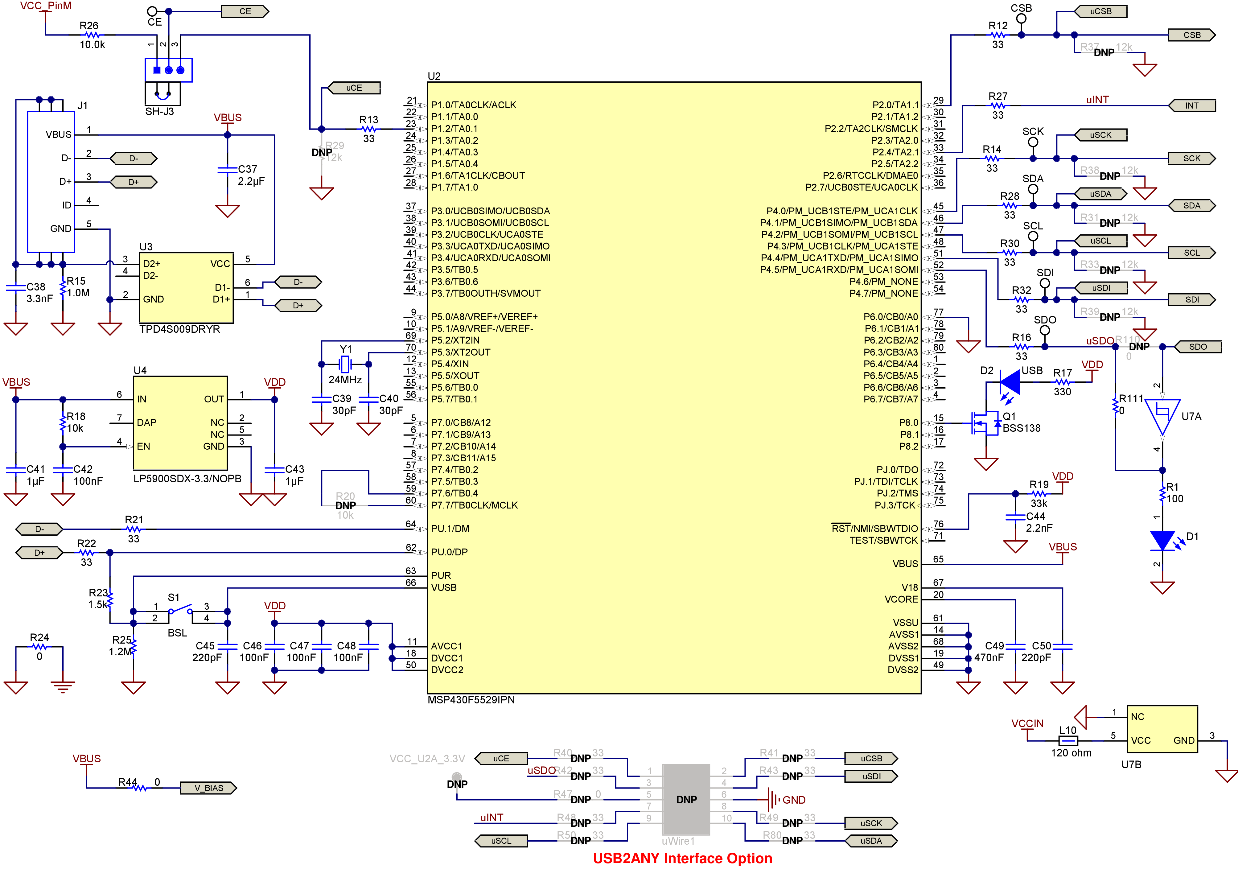
USB2ANY Interface