SNAU294 May 2024 LMX1205
4.1 Buffer Mode
After a POR or a soft reset, LMX1205 silicon default is buffer mode with all outputs enabled with maximum output power. LOGICLK is also enabled in this mode with a fixed divider value of 64. All SYSREF clocks are disabled. To evaluate the device in a different configuration, use TICS Pro.
From the top-menu, click Default Configuration → 3200MHz Buffer Mode. This automatically loads the buffer mode profile.
 Figure 4-1 Buffer Mode
If termination is not applied on all output pins, then manually disable the unused outputs using the CHx_EN fields (to completely power down unused channels) or the CLKOUTx_EN fields (to power down output buffers only). Powering down unused channels greatly reduces current consumption.
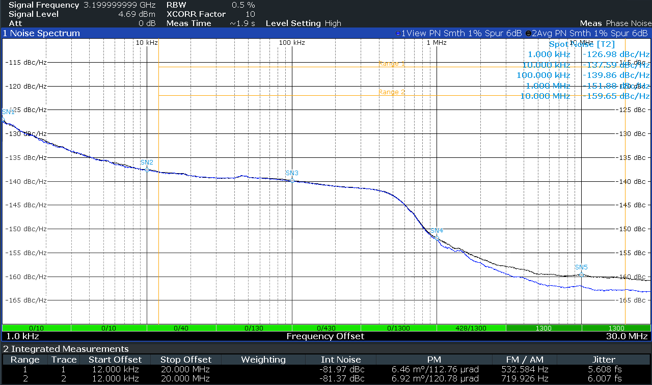
After the profile is loaded and required any changes have been made, click USB Communications → Write All Registers to program the device. In all of the following plots, the blue trace is the 3.2GHz reference clock from SMA100B and the black trace is the output clock from the device.
 Figure 4-2 Buffer Mode Output