SNAU306 June   2024 LMKDB1104


  1.   1
  2.   Description
  3.   Features
  4.   Applications
  5.   5
  6. 1Evaluation Module Overview
    1. 1.1 Introduction
    2. 1.2 Kit Contents
    3. 1.3 Specification
    4. 1.4 Device Information
  7. 2EVM Quick Start
    1. 2.1 Hardware Setup
    2. 2.2 Software Setup
      1. 2.2.1 TICS Pro GUI Setup
      2. 2.2.2 Power Up Sequence
    3. 2.3 EVM Measurements
  8. 3Hardware
    1. 3.1 Device Operation Modes
    2. 3.2 EVM Configuration
      1. 3.2.1 Power Supply
      2. 3.2.2 Logic Input and Outputs
      3. 3.2.3 Clock Input
      4. 3.2.4 Clock Outputs
      5. 3.2.5 Status Outputs, LEDs and Test Points
  9. 4Software
    1. 4.1 TICS Pro LMKDB1104 Software
      1. 4.1.1 Input
        1. 4.1.1.1 Input Interface Type
        2. 4.1.1.2 Input Termination
        3. 4.1.1.3 Auto Output Disable (AOD)
        4. 4.1.1.4 LOS Event
        5. 4.1.1.5 LOS Readback
      2. 4.1.2 Device Info and EVM Setup
        1. 4.1.2.1 Device Info
        2. 4.1.2.2 EVM Setup
        3. 4.1.2.3 SMBus
      3. 4.1.3 Output
        1. 4.1.3.1 SMBus
          1. 4.1.3.1.1 Programmable Output Slew Rate Control
        2. 4.1.3.2 OE Pins and Slew Rate Control
        3. 4.1.3.3 Side Band Interface (SBI)
  10. 5Implementation Results
    1. 5.1 Typical Phase Noise Characteristic
  11. 6Hardware Design Files
    1. 6.1 Schematics
    2. 6.2 PCB Layouts
    3. 6.3 Bill of Materials (BOM)
  12. 7Compliance Information
    1. 7.1 Compliance and Certifications
  13. 8Additional Information
    1. 8.1 Trademarks
  14. 9References

Schematics

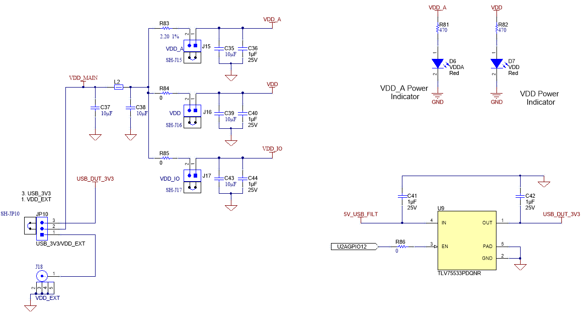
LMKDB1104EVM Power Supply (External and USB
          option) Figure 6-1 Power Supply (External and USB option)
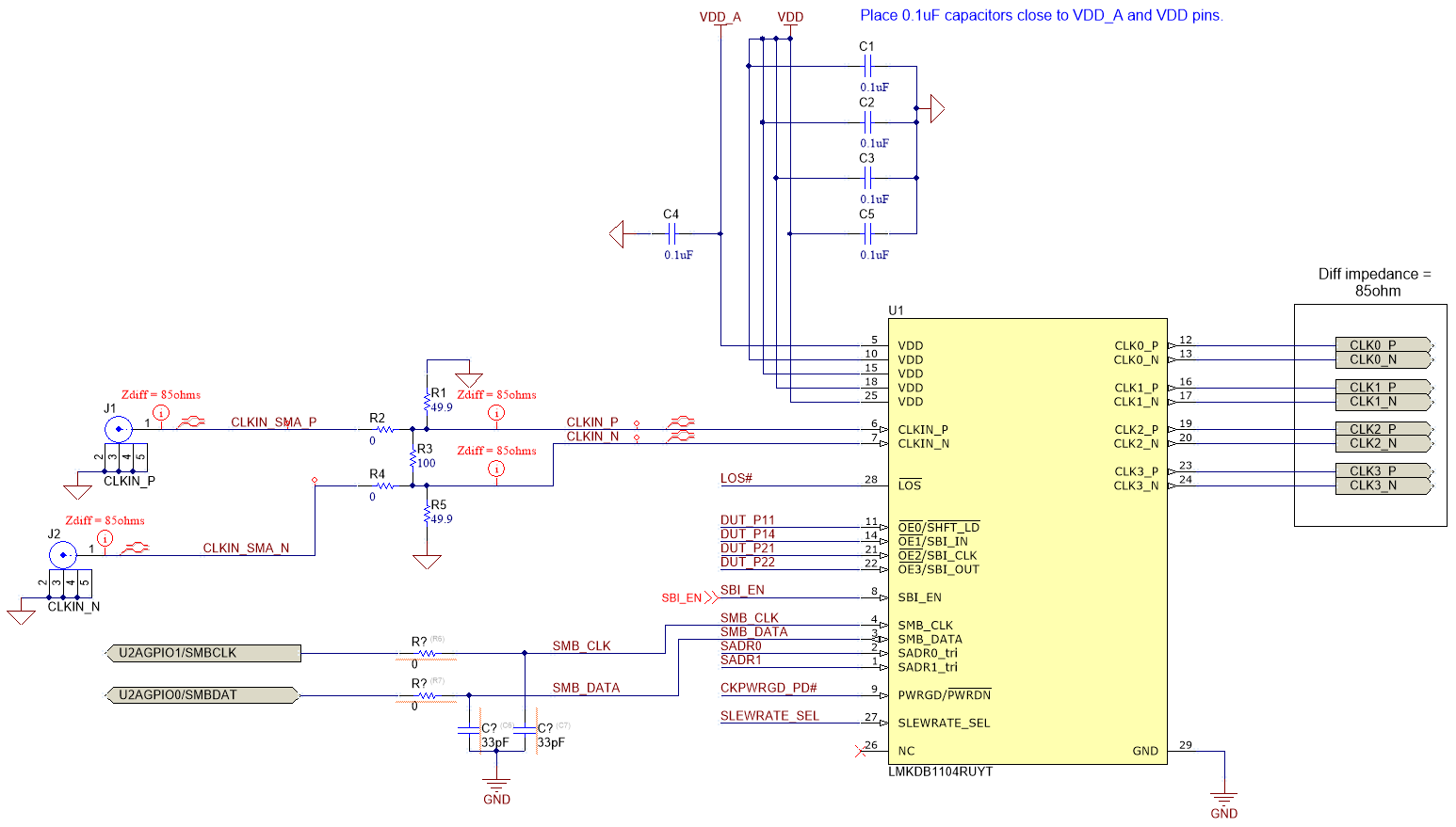
LMKDB1104EVM LMKDB1104 Device and CLKIN_P/N
          Reference Figure 6-2 LMKDB1104 Device and CLKIN_P/N Reference
LMKDB1104EVM Clock Outputs CLK0 to CLK7 Figure 6-3 Clock Outputs CLK0 to CLK7
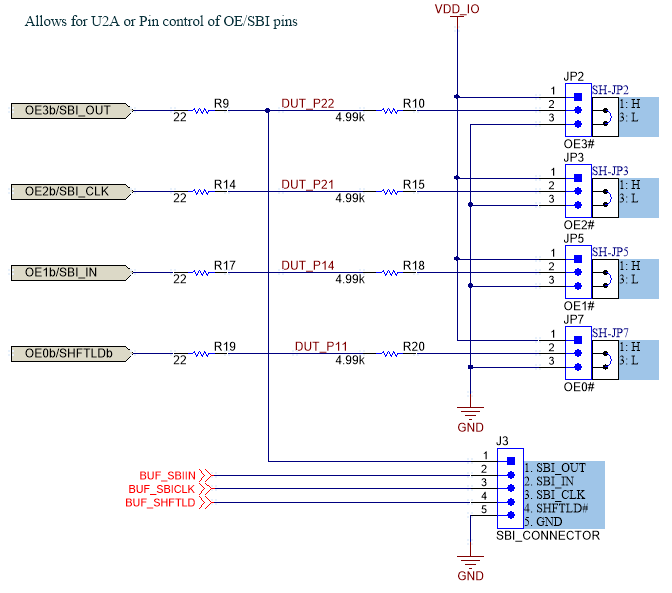
LMKDB1104EVM Output Enable Pins (OE#) Figure 6-4 Output Enable Pins (OE#)
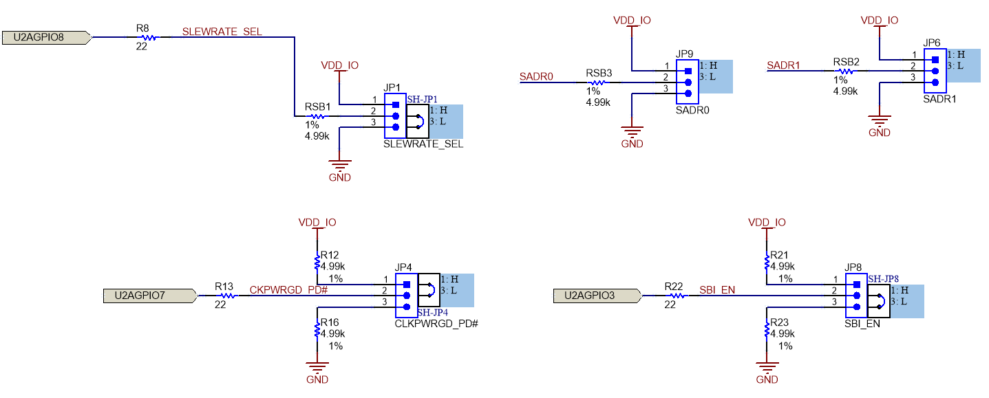
LMKDB1104EVM Logic I/O Jumpers Figure 6-5 Logic I/O Jumpers
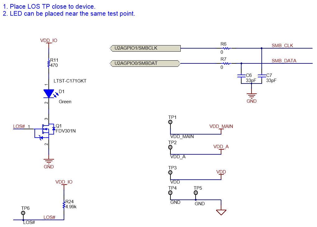
LMKDB1104EVM Status LEDs, Test Points, and SMBus
          Clock and Data Connections Figure 6-6 Status LEDs, Test Points, and SMBus Clock and Data Connections
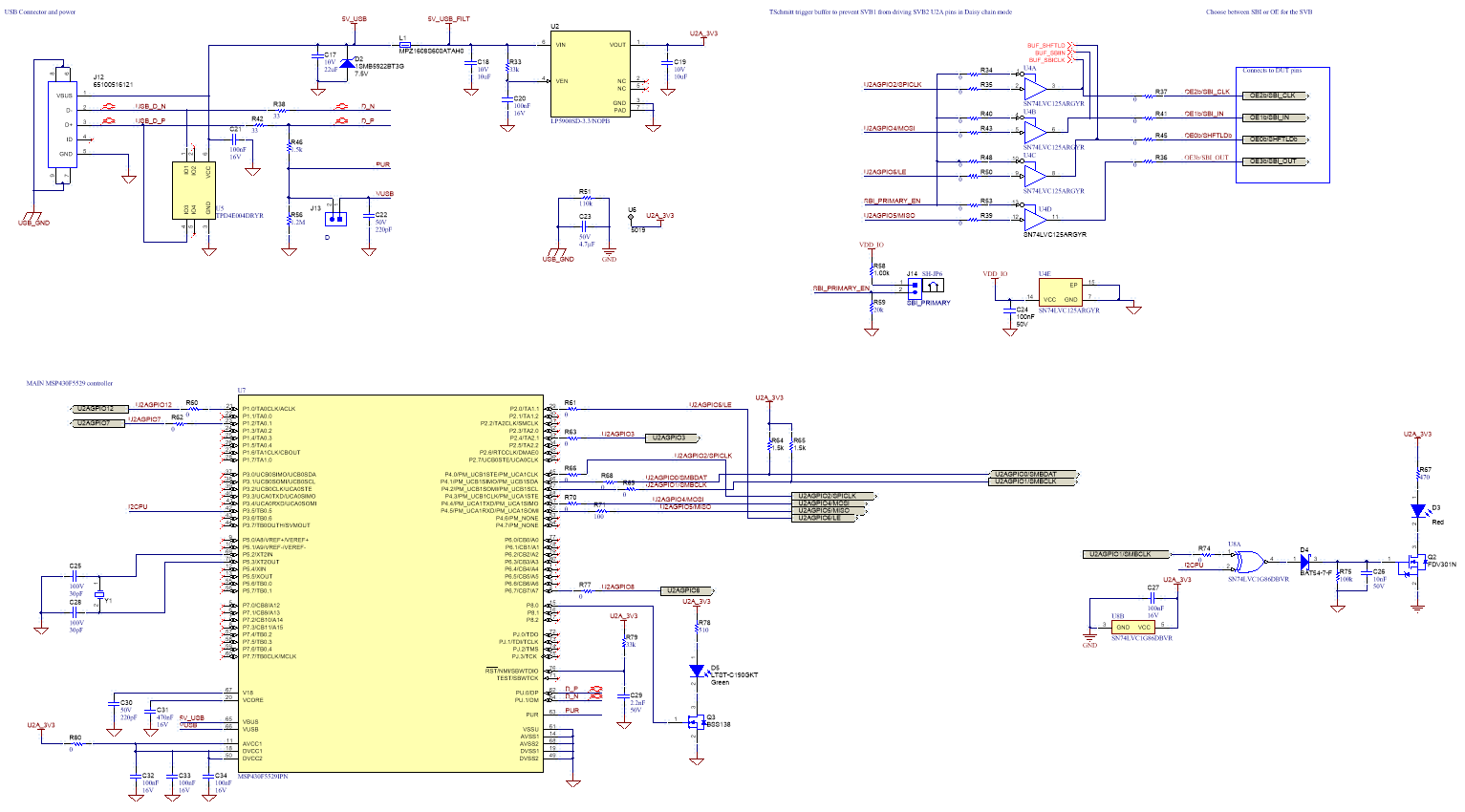
LMKDB1104EVM USB Schematic and Buffer Used for SBI
          and OE Pin Control Figure 6-7 USB Schematic and Buffer Used for SBI and OE Pin Control