SNLA224A June 2014 – January 2024 DS90UB913A-Q1 , DS90UB954-Q1 , DS90UB960-Q1
3.4 Layout Considerations
The layout of the PoC network is equally important as the network design. Due to the PoC network components making direct contact with the high-speed signal trace, good layout techniques and component placement are crucial to maintain signal integrity and remain within the insertion loss and return loss requirements. Both the high-speed channel and PoC network require tightly controlled 50-Ohms (+/-10%) impedance to minimize reflections. In addition to impedance, the PCB traces need to be thick enough to support the maximum expected current load.
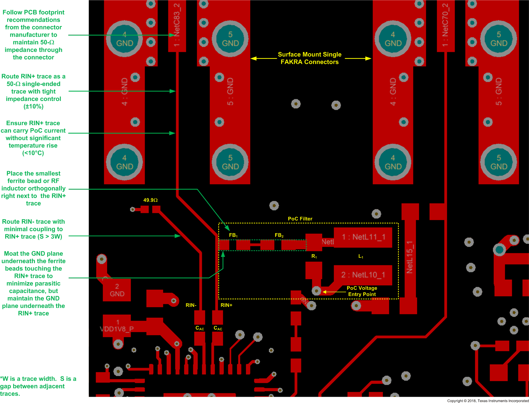
Place the first inductive component of the PoC network orthogonally to be barely touching the high-speed RIN+ trace. An anti-pad must be added under the first component to keep the impedance as close to 50-Ohms as possible. The anti-pad is created by adding a cut-out to the ground plane directly underneath the component’s landing pad. Since a continuous ground reference is required for the high-speed and PoC traces, the cut-out must not include any area under the connecting trace. Place the remaining PoC components close together to minimize the total footprint of the PoC network and limit 90-degree routing. For best EMI performance, do not route any high-frequency signals, including the PoC network, near the edge of the PCB board. Figure 3-1 shows an example PoC PCB layout with many of the previously described recommendations highlighted.
 Figure 3-1 Example PoC Layout and Routing
Keeping the entire PoC network on the same layer as the high-speed RIN+ trace is recommended since vias can result in impedance discontinuities. However, if space constraints arise, all components other than the first inductive component can be routed to a layer other than the layer with the high-speed trace. To maintain the 50-Ohm impedance, add ground reference vias near all signal vias. When sending signals between layers, care needs to be taken to avoid creating stubs. A stub is any transmission line that is only connected at one end. Stubs are commonly created by vias, routing, or through-hole connectors, which create reflections and degrade the signal quality.
For additional recommendations, refer to device data sheets.