SNLA267A March   2019  – June 2019 DS90UB953-Q1 , DS90UB954-Q1 , DS90UB960-Q1


  1.   How to Design a FPD-Link III System Using DS90UB953-Q1 and DS90UB954-Q1
    1.     Trademarks
    2. 1 Overview
      1. 1.1 System Level Functionality
    3. 2 Basic Design Rules
      1. 2.1 IDX and MODE Pin Verification
        1. 2.1.1 REF Clock, CLK IN, AON and Frequency Selection
          1. 2.1.1.1 Synchronous Mode
          2. 2.1.1.2 Non-Synchronous CLK_IN Mode
          3. 2.1.1.3 Non-Synchronous AON Mode
          4. 2.1.1.4 CSI Throughput
          5. 2.1.1.5 Clocking and Frequency Selection Example
      2. 2.2 Successful I2C Communication With 953 and 954
        1. 2.2.1 Aliasing
        2. 2.2.2 Port Selection on 954
      3. 2.3 I2C Passthrough Verification
      4. 2.4 Basic Diagnostic and Error Registers
    4. 3 Designing the Link Between SER and DES
      1. 3.1 Back Channel Configuration
      2. 3.2 BIST
        1. 3.2.1 BIST Configuration and Status
        2. 3.2.2 BIST Procedure
        3. 3.2.3 List of Registers Used in BIST Script
      3. 3.3 AEQ
      4. 3.4 CML Out
    5. 4 Designing Link Between SER and Image Sensor
      1. 4.1 Sensor Initialization Using SER GPIOs
      2. 4.2 CLKOUT
    6. 5 Designing Link Between DES and ISP
      1. 5.1 Frame Sync
        1. 5.1.1 Using SER GPIOs From the DES
        2. 5.1.2 Internal and External Frame Sync Configuration
        3. 5.1.3 Tables for Using GPIOs and Frame Sync
      2. 5.2 Port Forwarding
      3. 5.3 Pattern Generation
        1. 5.3.1 Accessing Indirect Registers
        2. 5.3.2 Pattern Generation From DES to ISP and SER to DES
    7. 6 Hardware Design
      1. 6.1 Basic I2C Connectors
        1. 6.1.1 I2C Pullups for SDA and SCL
      2. 6.2 AC Capacitor on FPD3 Link
      3. 6.3 Capacitance Used in Loop Filter
      4. 6.4 Critical Signal Routing
      5. 6.5 Time Domain Reflection
      6. 6.6 Return Loss and Insertion Loss
      7. 6.7 Power-over-Coax (PoC)
      8. 6.8 Voltage and Temperature Sensing
    8. 7 Appendix
      1. 7.1 Scripts
        1. 7.1.1  BIST Script
        2. 7.1.2  Example Sensor Initialization Script
        3. 7.1.3  CSI Enable and Port Forwarding Script
        4. 7.1.4  Enabling CMLOUT FPD3 RX Port 0 on 954
        5. 7.1.5  Remote Enabled SER GPIO Toggle Script
        6. 7.1.6  Local SER GPIO Toggle Script
        7. 7.1.7  Internal FrameSync on 953 GPIO1
        8. 7.1.8  External FrameSync on 953 GPIO0
        9. 7.1.9  SER GPIOs as Inputs and Output to DES GPIO
        10. 7.1.10 Pattern Generation on the 953 Script
        11. 7.1.11 Pattern Generation on the 954 Script
        12. 7.1.12 Monitor Errors for Predetermined Time Script
        13. 7.1.13 954 and 953 CSI Register Check Script
        14. 7.1.14 Time Till Lock Script on 953
      2. 7.2 Acknowledgments
  2.   Revision History

Basic Design Rules

This chapter describes a list of key items that are fundamental when powering on the system. These items define the functionality of the entire system. To get the system up and running quickly, TI recommends to check these items before moving forward.
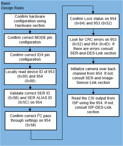
swru519_basic_design_rules.gifFigure 2. Basic Design Rules Flowchart