SNLA431 January 2024 DP83TC812R-Q1 , DP83TC812S-Q1
- 1
- Trademarks
- 1Preface
- Notational Conventions
- 2Related Documentation
- 3Support Resources
-
4Troubleshooting the PHY Application
- 4.1 Schematic and Layout Checklist
- 4.2 Verify Successful Power-up of PHY
- 4.3 Peripheral Pin Checks
- 4.4 Register Dump Comparison
- 4.5 Verifying Strap Configurations
- 4.6 Check the MDI Signal
- 4.7 Link Up Failed Common Issues
- 4.8 Signal Quality Check
- 4.9 Power Up Timing
- 4.10 Loopback Testing
- 4.11 Debugging the MAC Interface
- 4.12 Verify Open Alliance PMA Compliance
- 4.13 Tools and References
- 5Conclusion
4.3.4 Probe the Serial Management Interface (MDC, MDIO) Pins
If register read and write is successful, this section can be skipped.
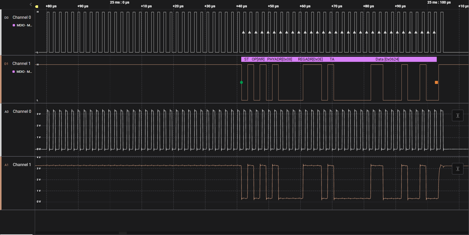
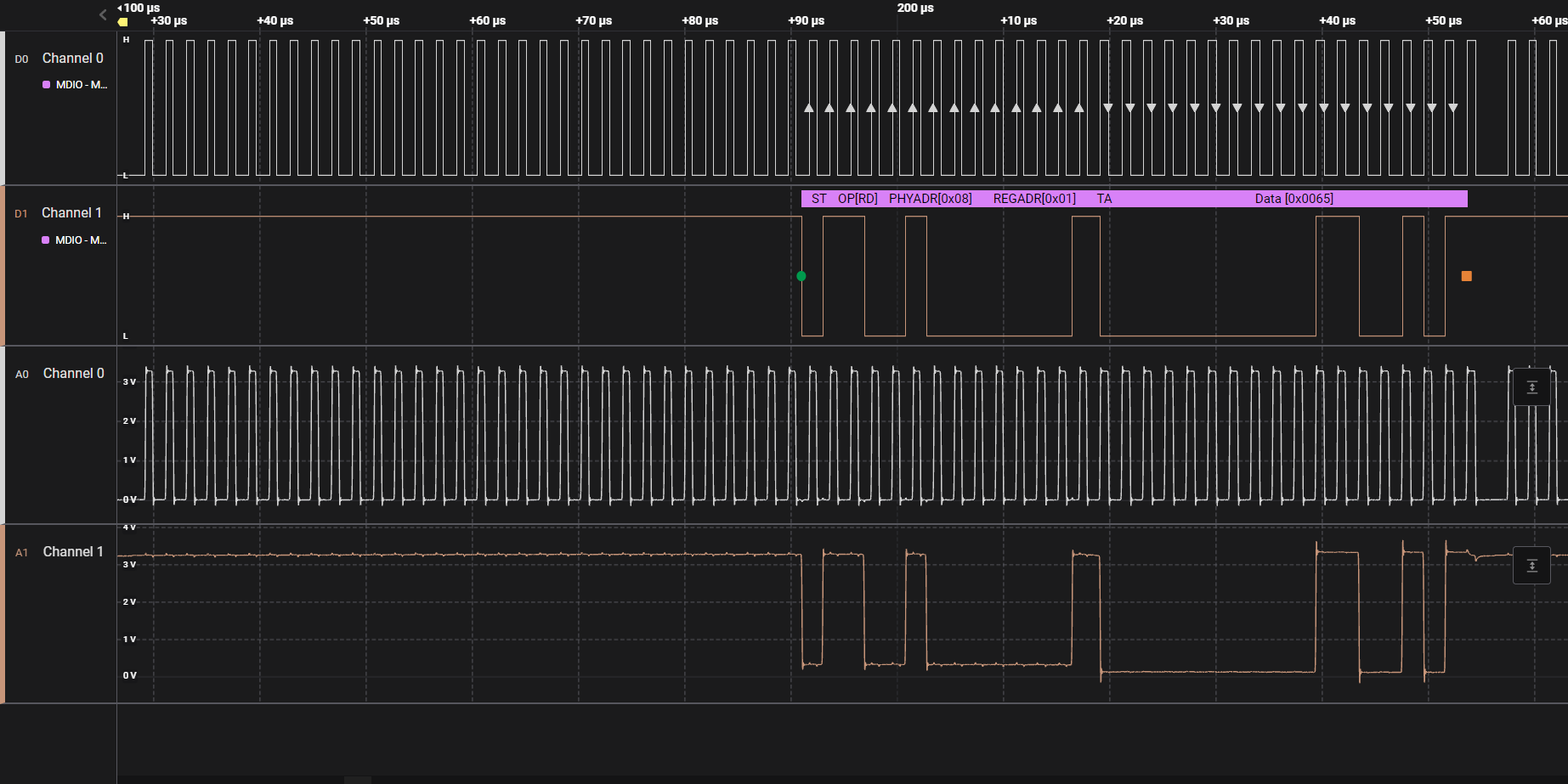
If register read and write is unsuccessful, probe the MDC signal (pin 1) to maintain that there is a ≤20Mhz clock signal being sourced from the MAC. Additionally, the MDIO signal (pin 36) can be decoded using a logic analyzer as shown below.
Note, to access extended registers (those beyond 0x1F), the procedure given in section 8.4.15 of the data sheet must be used.
|
SMI Protocol |
<idle><start><op code><device addr><reg addr><turnaround><data><idle> |
|---|---|
|
Read Register |
<idle><01><10><AAAAA><RRRRR><Z0><XXXX XXXX XXXX XXXX><idle> |
|
Write Register |
<idle><01><01><AAAAA><RRRRR><10><XXXX XXXX XXXX XXXX><idle> |
 Figure 4-2 MDC/MDIO Write Example
 Figure 4-3 MDC/MDIO Read Example