DS125BR111 Low Power 12.5 Gbps 1-Lane Linear Repeater with Equalization
1 Features
- Low 65 mW/Channel (typ) Power Consumption
- Supports Link Training
- Supports Out-of-Band (OOB) Signaling
- Advanced Signal Conditioning I/O
- Receive CTLE up to 10 dB at 6 GHz
- Linear Output Driver
- Output Voltage Range over 1200 mV
- Programmable via Pin Selection, EEPROM, or SMBus Interface
- Single Supply Voltage: 2.5 V or 3.3 V
- −40°C to 85°C Operating Temperature Range
- Flow-thru Pinout in 4 mm × 4 mm 24-pin Leadless WQFN Package
2 Applications
- SAS-1/2/3 and SATA-1/2/3
- PCI Express 1/2/3
- Other Proprietary Interfaces up to 12.5 Gbps
3 Description
The DS125BR111 is an extremely low power high performance repeater/redriver designed to support 1-lane carrying high speed interface up to 12.5 Gbps. The receiver's continuous time linear equalizer (CTLE) provides a boost of 3-10 dB at 6 GHz in each channel. When operating in SAS-3 or PCIe Gen-3 applications, the DS125BR111 preserves transmit signal characteristics allowing the host controller and the end point to negotiate transmit equalizer coefficients. Transparency to the link training protocol maximizes the flexibility of the physical placement of the device within the interconnect and improves overall channel performance.
The programmable settings can be applied easily via pins, software (SMBus or I2C), or loaded via an external EEPROM. In EEPROM mode, the configuration information is automatically loaded on power up, which eliminates the need for an external microprocessor or software driver.
Device Information(1)
| PART NUMBER | PACKAGE | BODY SIZE (NOM) |
|---|---|---|
| DS125BR111 | WQFN (24) | 4.00mm x 4.00mm |
- For all available packages, see the orderable addendum at the end of the datasheet.
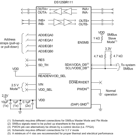
4 Simplified Schematic
5 Revision History
Changes from B Revision (July 2014) to C Revision
- Changed data sheet flow and layout to conform with new TI standards. Added the following sections: Application and Implementation; Power Supply Recommendations; Layout; Device and Documentation Support; Mechanical, Packaging, and Ordering Information Go
Changes from A Revision (January 2014) to B Revision
- Changed Features Go
Changes from * Revision (April 2013) to A Revision
- Changed layout of National Data Sheet to TI formatGo
6 Pin Configuration and Functions

The center DAP on the package bottom is the only device GND connection. This pad must be connected to GND through multiple (minimum of 4) vias to ensure optimal electrical and thermal performance.
Pin Functions
| PIN | I/O | DESCRIPTION | |
|---|---|---|---|
| NAME | NO. | ||
| DIFFERENTIAL HIGH SPEED I/O | |||
| INB+, INB- | 11, 12 | I | Inverting and non-inverting CML differential inputs to the equalizer. On-chip 50 Ω termination resistor connects INB+ to VDD and INB- to VDD when enabled by RXDET control logic. AC coupling required on high-speed I/O |
| OUTB+, OUTB- | 20, 19 | O | Inverting and non-inverting 50 Ω driver outputs. Compatible with AC coupled CML inputs. AC coupling required on high-speed I/O |
| INA+, INA- | 24, 23 | I | Inverting and non-inverting CML differential inputs to the equalizer. On-chip 50 Ω termination resistor connects INA+ to VDD and INA- to VDD when enabled by RXDET control logic. AC coupling required on high-speed I/O |
| OUTA+, OUTA- | 7, 8 | O | Inverting and non-inverting 50 Ω driver outputs. Compatible with AC coupled CML inputs. AC coupling required on high-speed I/O |
| CONTROL PINS — SHARED (LVCMOS) | |||
| ENSMB | 3 | I, 4-LEVEL, LVCMOS |
System Management Bus (SMBus) enable Pin Tie 1 kΩ to VDD = Register Access SMBus Slave mode FLOAT = Read External EEPROM (Master SMBus Mode) Tie 1 kΩ to GND = Pin Mode |
| ENSMB = Float or 1 (SMBus MODEs) | |||
| SCL | 5 | I, LVCMOS, O, OPEN Drain |
ENSMB Master or Slave mode SMBus clock input Pin is enabled (slave mode). Clock output when loading EEPROM configuration (master mode). |
| SDA | 4 | I, LVCMOS, O, OPEN Drain |
ENSMB Master or Slave mode The SMBus bidirectional SDA Pin is enabled. Data input or open drain output. External pull-up required as per SMBus protocol (typically in the 2 kΩ to 5 kΩ range). This pin is 3.3 V-tolerant. |
| AD0-AD3 | 10, 9, 2, 1 | I, LVCMOS | ENSMB Master or Slave mode SMBus Slave Address Inputs. In SMBus mode, these Pins are the user set SMBus slave address inputs. |
| READEN | 17 | I, LVCMOS | ENSMB = Float: When using an External EEPROM, a logic low on this pin starts the load from the external EEPROM ENSMB = 1: When using SMBus Slave Mode the VOD_SEL/READEN pin must be tied Low for the AD[3:0] to be active. If this pin is tied High or Floated an address of 0xB0 will be used for the DS125BR111. |
| DONE | 18 | O, LVCMOS | When using an External EEPROM (ENSMB = Float), Valid Register Load Status Output HIGH = External EEPROM load failed or incomplete LOW = External EEPROM load passed |
| ENSMB = 0 (PIN MODE) | |||
| EQA0 EQB0 |
10 1 |
I, 4-LEVEL, LVCMOS |
EQA0 and EQB0 control the level of equalization of the A/B directions. The Pins are defined as EQx0 only when ENSMB is de-asserted (low). When ENSMB goes high the SMBus registers provide independent control of each channel. See Table 4. |
| EQA1 EQB1 |
9 2 |
I, 4-LEVEL, LVCMOS |
EQA1 and EQB1 are not used in the DS125BR111 design. These pins should always be tied to GND. |
| VODA_DB | 4 | I, 4-LEVEL, LVCMOS |
VODA_DB controls the CHA output amplitude dynamic range, for SAS and PCIe applications it should be held Low. The Pin is defined as VODA_DB only when ENSMB is de-asserted (low). When ENSMB goes high the SMBus registers provide control of each channel, pin 4 is converted to SDA. See Table 5. |
| VODB_DB | 5 | I, 4-LEVEL, LVCMOS |
VODB_DB controls the CHB output amplitude dynamic range, for SAS and PCIe applications it should be held Low. The Pin is defined as VODB_DB only when ENSMB is de-asserted (low). When ENSMB goes high the SMBus registers provide control of each channel, pin 5 is converted to SCL. See Table 5. |
| SD_TH | 14 | I, 4-LEVEL, LVCMOS |
Controls the internal Signal Detect Threshold. This detection threshold is for system debug only and does not control the high speed datapath. See Table 3. |
| VOD_SEL | 17 | I, 4-LEVEL, LVCMOS |
VOD_SEL controls the low frequency ratio of input voltage to output voltage amplitude. See Table 5. |
| RXDET | 18 | I, 4-LEVEL, LVCMOS |
The RXDET Pin controls the receiver detect function. Depending on the input level, a 50 Ω or > 50 kΩ termination to the power rail is enabled. In a SAS/SATA system RXDET should be set to a Logic "1" state to keep the termination always enabled. The RXDET pin only controls the RXDET function in PIN MODE. PCIe applications which require SMBus Mode functionality must utilize a specific register write sequence documented in PCIe Applications . If this sequence is not utilized, SMBus configuration modes will default the input terminations to active (50 Ω). See Table 2 . |
| CONTROL PINS — BOTH PIN AND SMBus MODES (LVCMOS) | |||
| RES | 13 | I, 4-LEVEL, LVCMOS |
Reserved: This input must be left Floating. |
| VDD_SEL | 16 | I, FLOAT | Controls the internal regulator Float = 2.5 V mode Tie GND = 3.3 V mode |
| PWDN | 6 | I, LVCMOS | Tie High = Low power - power down Tie GND = Normal Operation See Table 2. |
| POWER (See Figure 11) | |||
| VIN | 15 | Power | In 3.3 V mode, feed 3.3 V to VIN In 2.5 V mode, leave floating. |
| VDD | 21, 22 | Power | Power supply pins CML/analog 2.5 V mode, connect to 2.5 V 3.3 V mode, decouple each VDD pin with 0.22 µF cap to GND |
| GND | DAP | Power | Ground pad (DAP - die attach pad). |