SNLS512 April 2016 DS90UB924-Q1
PRODUCTION DATA.
- 1 Features
- 2 Applications
- 3 Description
- 4 Revision History
- 5 Pin Configuration and Functions
-
6 Specifications
- 6.1 Absolute Maximum Ratings
- 6.2 ESD Ratings
- 6.3 Recommended Operating Conditions
- 6.4 Thermal Information
- 6.5 DC Electrical Characteristics
- 6.6 AC Electrical Characteristics
- 6.7 DC and AC Serial Control Bus Characteristics
- 6.8 Timing Requirements for the Serial Control Bus
- 6.9 Timing Requirements
- 6.10 Typical Characteristics
-
7 Detailed Description
- 7.1 Overview
- 7.2 Functional Block Diagram
- 7.3
Feature Description
- 7.3.1 High-Speed Forward Channel Data Transfer
- 7.3.2 Low-Speed Back Channel Data Transfer
- 7.3.3 Backward Compatible Mode
- 7.3.4 Input Equalization
- 7.3.5 Common Mode Filter Pin (CMF)
- 7.3.6 Power Down (PDB)
- 7.3.7 Video Control Signals
- 7.3.8 EMI Reduction Features
- 7.3.9 Built In Self Test (BIST)
- 7.3.10 Internal Pattern Generation
- 7.3.11 Serial Link Fault Detect
- 7.3.12 Oscillator Output
- 7.3.13 Interrupt Pin (INTB / INTB_IN)
- 7.3.14 General-Purpose I/O
- 7.3.15 I2S Audio Interface
- 7.3.16 AV Mute Prevention
- 7.3.17 OEN Toggling Limitation
- 7.4 Device Functional Modes
- 7.5 Programming
- 7.6 Register Maps
- 8 Application and Implementation
- 9 Power Supply Recommendations
- 10Layout
- 11Device and Documentation Support
- 12Mechanical, Packaging, and Orderable Information
8 Application and Implementation
NOTE
Information in the following applications sections is not part of the TI component specification, and TI does not warrant its accuracy or completeness. TI’s customers are responsible for determining suitability of components for their purposes. Customers must validate and test their design implementation to confirm system functionality.
8.1 Application Information
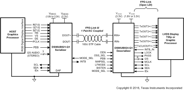
The DS90UB924-Q1 deserializer, in conjunction with a DS90UB921-Q1, DS90UB925Q-Q1 or DS90UB927Q-Q1 serializer, provides a solution for distribution of digital video and audio within automotive infotainment systems. It converts a high-speed serialized interface with an embedded clock, delivered over a single signal pair (FPD-Link III), to four LVDS data/control streams, one LVDS clock pair (FPD-Link (OpenLDI)), and I2S audio data. The serial bus scheme, FPD-Link III, supports high-speed forward channel data transmission, and low-speed full duplex back channel communication over a single differential link. Consolidation of audio, video data, and control over a single differential pair reduces the interconnect size and weight, while also eliminating skew issues and simplifying system design.
8.2 Typical Application
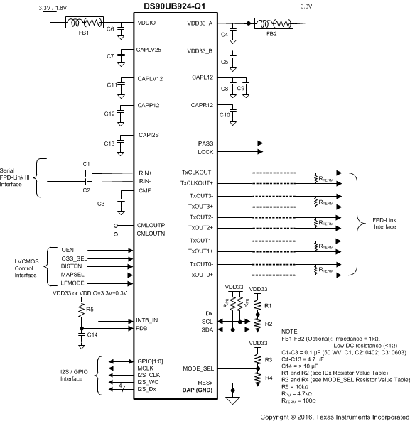
Figure 37 shows a typical application of the DS90UB924-Q1 deserializer for an 96 MHz 24-bit color display application. Inputs utilize 0.1-µF coupling capacitors to the line, and the deserializer provides internal termination. The voltage rating of the coupling capacitors must be ≥50 V and must use a small body capacitor size, such as 0402 or 0602, to help ensure good signal integrity. The FPD-Link (OpenLDI) LVDS differential outputs require 100-Ω termination resistors at the receiving device or display.
Bypass capacitors must be placed near the power supply pins. At a minimum, three 4.7-μF capacitors, one placed at each power supply pin, are required for local device bypassing. If additional bypass capacitors are used, place the smaller value components closer to the pin. Ferrite beads are required on the two supplies (VDD33 and VDDIO) for effective noise suppression. Connect pins VDD33_A and VDD33_B directly to ensure ESD performance. The interface to the display is FPD-Link (OpenLDI) LVDS. The VDDIO pin may be connected to 3.3 V or 1.8 V. Place a delay capacitor (>10 µF) and pullup resistor (10 kΩ) on the PDB signal to delay the enabling of the device until power is stable.
 Figure 37. Typical Connection Diagram
 Figure 38. Typical Display System Diagram
8.2.1 Design Requirements
For the typical design application, use the following as input parameters:
Table 9. Design Parameters
| DESIGN PARAMETER | EXAMPLE VALUE |
|---|---|
| VDDIO | 1.8 V or 3.3 V |
| VDD33 | 3.3 V |
| AC Coupling Capacitor for RIN± | 330nF for RIN+, 250nF for RIN- (Single-ended) 100 nF for RIN+/- (Differential) |
| PCLK Frequency | 96 MHz |
8.2.2 Detailed Design Procedure
8.2.2.1 Transmission Media
The DS90UB927Q-Q1/DS90UB921-Q1/DS90UB925Q-Q1 and DS90UB924-Q1 chipset is intended to be used in a point-to-point configuration through a shielded twisted pair cable. The serializer and deserializer provide internal termination to minimize impedance discontinuities. The interconnect (cable and connector) between the serializer and deserializer must have a differential impedance of 100 Ω. The maximum length of cable that can be used is dependant on the quality of the cable (gauge, impedance), connector, board (discontinuities, power plane), the electrical environment (for example, power stability, ground noise, input clock jitter, PCLK frequency, and so forth.) and the application environment.
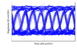
The resulting signal quality at the receiving end of the transmission media may be assessed by monitoring the differential eye opening of the serial data stream. The Receiver CML Monitor Driver Output Specifications define the acceptable data eye opening width and eye opening height. use a differential probe to measure across the termination resistor at the CMLOUTP/CMLOUTN pins.
8.2.2.2 Display Application
The DS90UB924-Q1, in conjunction with the DS90UB921-Q1, is intended for interfacing with a host (graphics processor) and a display supporting 24-bit color depth (RGB888) and high-definition (720p) digital video format. It can receive an 8-bit RGB stream with a pixel clock rate up to 96 MHz together with three control bits (VS, HS, and DE) and four I2S audio streams.
8.2.3 Application Curves
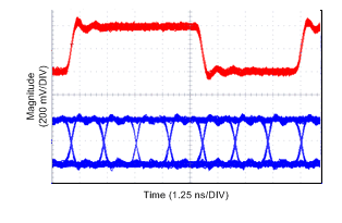
 Figure 39. 96 MHz TxCLKOUT± and TxOUT0± Data Output
 Figure 40. CMLOUT of Deserializer from 96 MHz Input Clock