SNOAA89 December 2022 AM2431 , AM2432 , AM2434
2.3 Verification
To verify the mechanism for FSI data transferring using the ICSSG module, the code on the LP-AM243 is tested. Figure 2-6 shows the test set up.
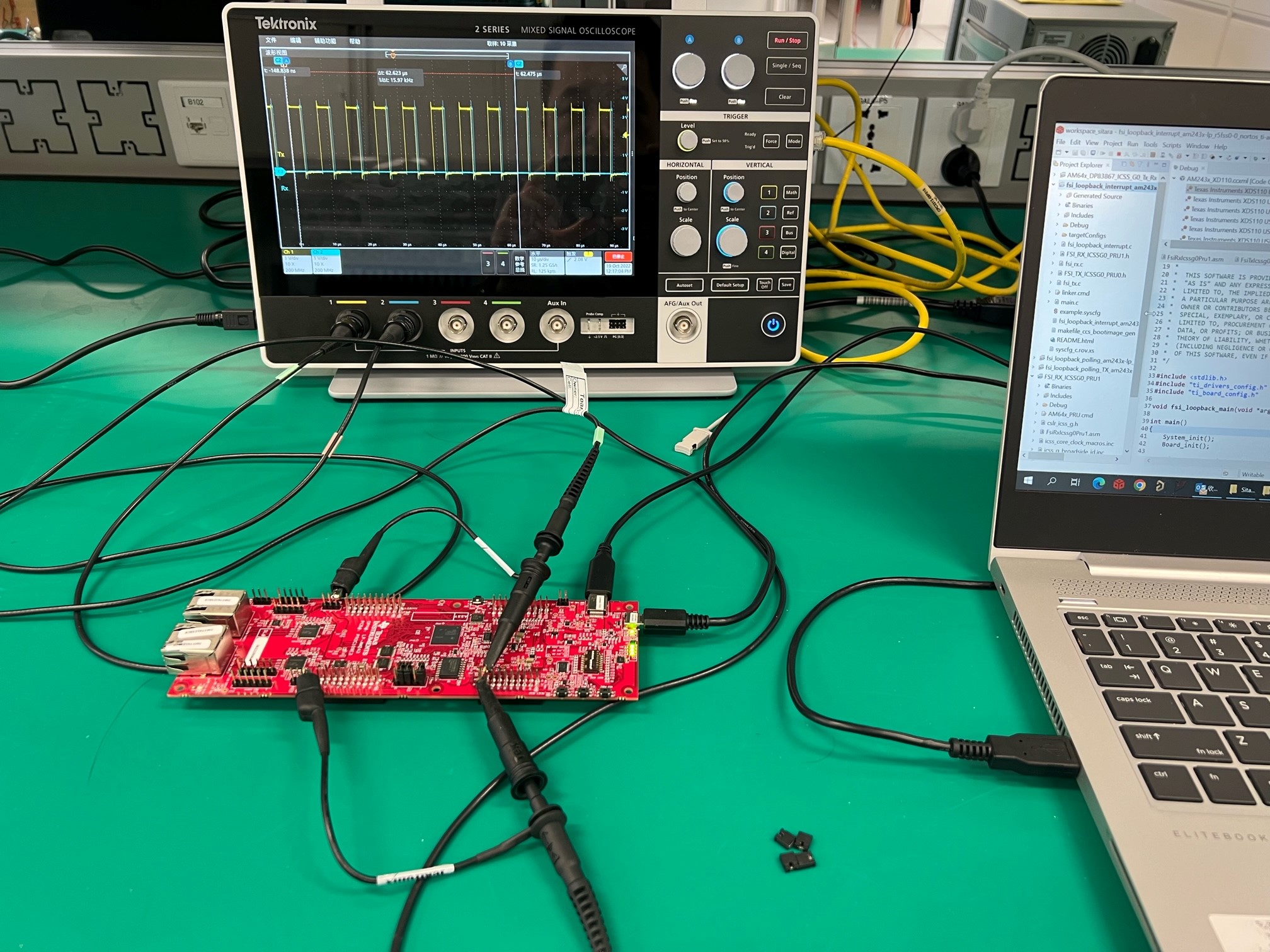 Figure 2-6 Test Set up
The AM243x LaunchPad™ provides an FSI header with FSI_TX0 and FSI_RX0 channels. To perform external loopback communication, jumper the two data lines and clock signals as Figure 2-7 shows.
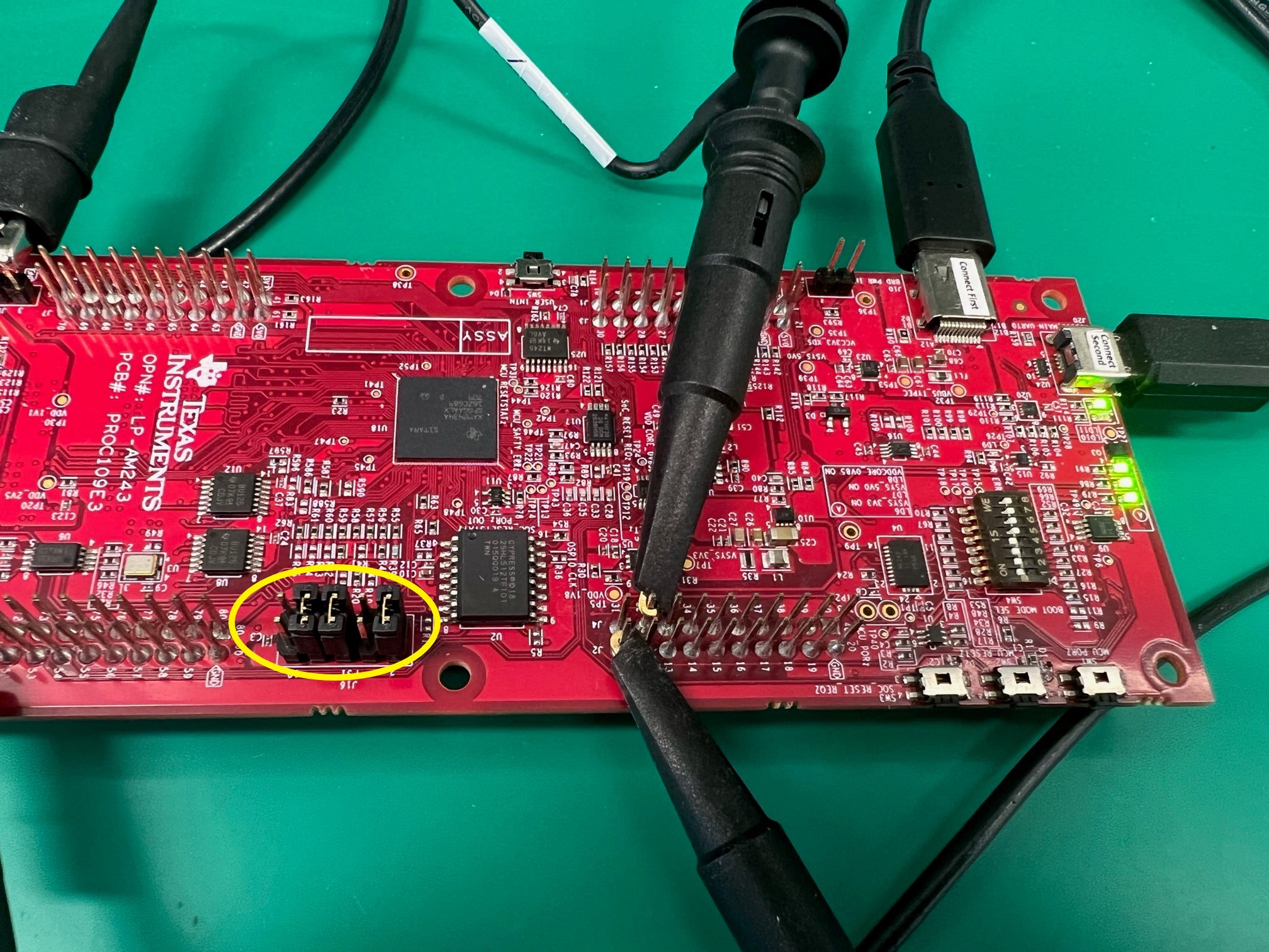 Figure 2-7 Jumper the Two Data Lines and
Clock Signals
Figure 2-7 Jumper the Two Data Lines and
Clock SignalsThe test conditions for R5 core control:
→ TX, RX module configuration with handshake
|
#define FSI_APP_TXCLK_FREQ (50 * 1000 * 1000) #define FSI_APP_CLK_FREQ (CONFIG_FSI_TX0_CLK) #define FSI_APP_TX_PRESCALER_VAL (FSI_APP_CLK_FREQ / FSI_APP_TXCLK_FREQ / 2U) #define FSI_APP_N_LANES (0x1U) #define FSI_APP_FRAME_DATA_WORD_SIZE (16U) FSI_executeTxFlushSequence(txBaseAddr, FSI_APP_TX_PRESCALER_VAL); |
→ FSI TX0 transmitting data (16 Length 16-bit words) from MSRAM to TX buffer, clear TX event
→ CLK and data from TX to RX with jumper
→ Check if RX buffer frame done, write data from RX buffer to MSRAM, clear RX event
Two GPOs are configured accordingly for TX and RX.
For the TX part, GPO0 is set high when the TX buffer is going to set and set low after TX event is cleared and data transfer is done.
For the RX part, GPO1 is set high after the TX event is cleared and set low when data transfer is done.
The test conditions for PRU handler:
→ TX, RX module configuration with handshake
→ FSI TX0 transmitting data (16 Length 16-bit words) from TCM to TX buffer using PRU_XFR2VBUS, clear TX event
→ CLK and data from TX to RX with jumper
→ RX event trigger PRU INTC and data movement from the RX buffer to TCM, clear RX event
Two GPOs are configured accordingly for TX and RX.
For the TX part, GPO0 is set high when the TX buffer is going to set and set low after TX event is cleared and data transfer is done.
For the RX part, GPO1 is set high when receive interrupt flag is set in PRU INTC and set low when data transfer is done.
Test results:
The compare value of IEP timer to trigger transmitting are set with 8 × 7.8 µs = 62.5 µs (16-kHz communication cycle). Figure 2-8 shows the verification waveform.
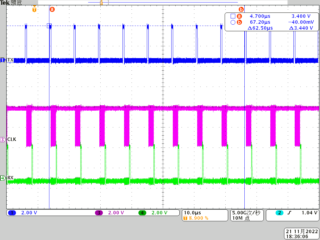 Figure 2-8 Communication Cycle
Table 2-1 shows the comparison results between the R5 core control and PRU handler on FSI communication. From the test results, the PRU handler helps to have 6 times reduction in FSI processing time (RX + TX) from 4.42 µs to 740 ns. And the time obtained for the data transmission is about 1.6 µs. To calculate the transmission speed, the consider the total data length. Figure 1-3 shows the general structure of a data frame, which can be divided into two parts: effective data bits and overhead bits.
- Effective Data Bits: Includes the 8-bit user data, 16-bit data words, and 8-bit CRC fields
- Overhead Bits: Includes the Preamble, SOF, Frame Type, EOF, and Epilogue fields
Since two data lines only work for effective data bits, one FSITXCLK cycle delivers 4 effective data bits, while one FSITXCLK cycle only delivers 2 overhead bits.
Therefore, the best transmission time for 16 words can be derived theoretically as follows:
- Effective data bits = 16-bits × 16 (data words) + 8-bits (user data) + 8-bits (CRC) =272 bits
- Total Length bits = Effective data + Overhead = 272 + 24 = 296 bits
- FSITXCLK cycles for total Length = 272/4 + 24/2 = 80 cycles
Thus, with a total 80 FSITXCLK cycles for 16 data words, the transmission time can be calculated as follows:
(FSITXCLK cycles) / (FSITXCLK frequency) = 80 / 50 MHz = 1.6 µs (Conforms to the test results).
So, the transmission speed is 185Mbps (296 / 1.6 µs).
| Controller | FSITXCLK (MHz) | Data Lines | Data Length (Bit) | TX Module Data Processing Time (µs) | Transmission Time (µs) | RX Module Data Processing Time (µs) | Total Time (µs) |
|---|---|---|---|---|---|---|---|
| R5 Core Control |
50 |
2 |
16 |
1.5 |
1.6 |
2.92 |
6.5(1) |
|
PRU Handler |
50 |
2 |
16 |
0.46 |
1.6 |
0.28 |
2.396(1) |
Figure 2-9–Figure 2-16 show the test waveforms including total cycle time, transmit latency, data transfer, and receive latency comparison between R5 core control and PRU handler.
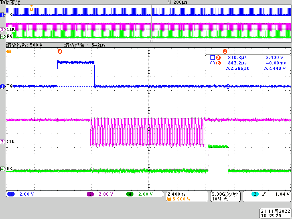 Figure 2-9 PRU handler_total Cycle
Time
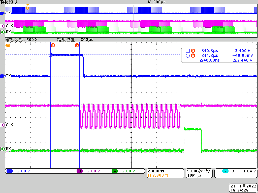 Figure 2-11 PRU handler_Transmit
Latency
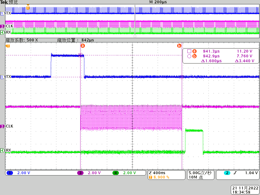 Figure 2-13 PRU handler_Data Transfer
 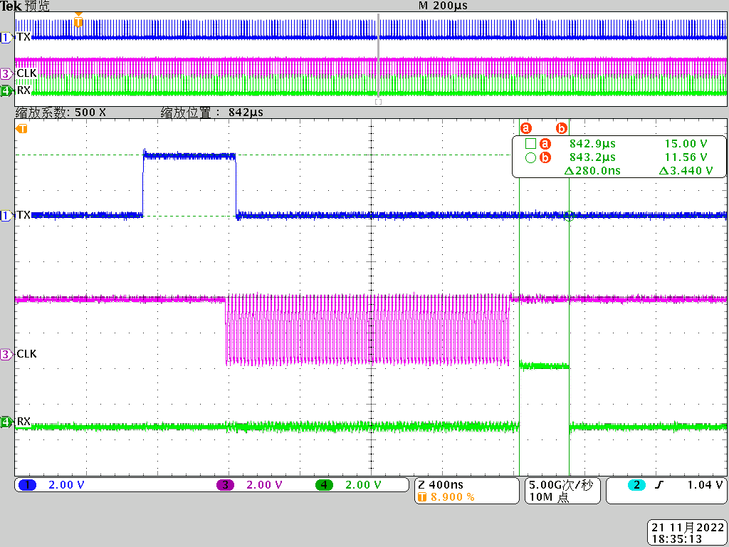 Figure 2-15 PRU handler_Receive
Latency
 Figure 2-10 R5 Core control_total
Cycle Time
 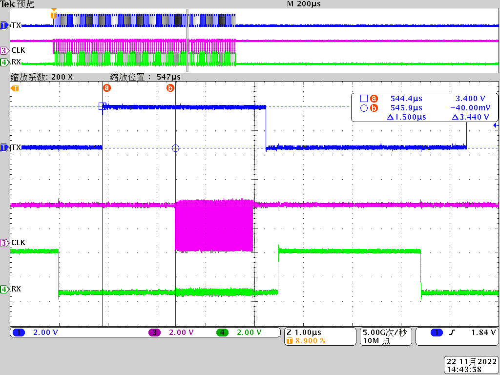 Figure 2-12 R5 Core control_Transmit
Latency
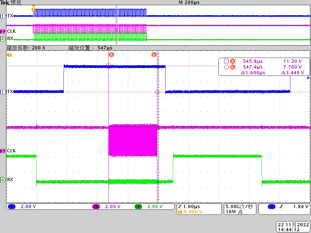 Figure 2-14 R5 Core control_Data
Transfer
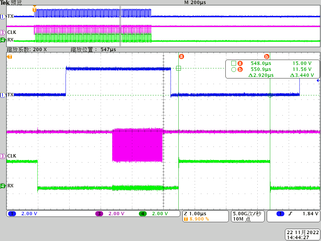 Figure 2-16 R5 Core control_Receive
Latency