SNOSD91B March   2019  – February 2020

PRODUCTION DATA.  

  1. Features
  2. Applications
  3. Description
    1.     Device Images
      1.      Simplified Block Diagram
      2.      Switching Performance
  4. Revision History
  5. Pin Configuration and Functions
    1.     Pin Functions
  6. Specifications
    1. 6.1 Absolute Maximum Ratings
    2. 6.2 ESD Ratings
    3. 6.3 Recommended Operating Conditions
    4. 6.4 Thermal Information
    5. 6.5 Electrical Characteristics
    6. 6.6 Switching Characteristics
    7. 6.7 Typical Characteristics
  7. Parameter Measurement Information
    1. 7.1 Switching Parameters
    2. 7.2 Turn-on Delays
    3. 7.3 Turn-off Delays
    4. 7.4 Drain Slew Rate
  8. Detailed Description
    1. 8.1 Overview
    2. 8.2 Functional Block Diagram
    3. 8.3 Feature Description
      1. 8.3.1 Direct-Drive GaN Architecture
      2. 8.3.2 Internal Buck-Boost DC-DC Converter
      3. 8.3.3 Internal Auxiliary LDO
      4. 8.3.4 Start Up Sequence
      5. 8.3.5 R-C Decoupling for IN pin
      6. 8.3.6 Low Power Mode
      7. 8.3.7 Fault Detection
        1. 8.3.7.1 Overcurrent Protection
        2. 8.3.7.2 Over-Temperature Protection and UVLO
      8. 8.3.8 Drive Strength Adjustment
    4. 8.4 Safe Operation Area (SOA)
      1. 8.4.1 Repetitive SOA
  9. Application and Implementation
    1. 9.1 Application Information
    2. 9.2 Typical Application
      1. 9.2.1 Design Requirements
      2. 9.2.2 Detailed Design Procedure
        1. 9.2.2.1 Slew Rate Selection
          1. 9.2.2.1.1 Startup and Slew Rate with Bootstrap High-Side Supply
        2. 9.2.2.2 Signal Level-Shifting
        3. 9.2.2.3 Buck-Boost Converter Design
    3. 9.3 Dos and Don'ts
  10. 10Power Supply Recommendations
    1. 10.1 Using an Isolated Power Supply
    2. 10.2 Using a Bootstrap Diode
      1. 10.2.1 Diode Selection
      2. 10.2.2 Managing the Bootstrap Voltage
      3. 10.2.3 Reliable Bootstrap Start-up
  11. 11Layout
    1. 11.1 Layout Guidelines
      1. 11.1.1 Power Loop Inductance
      2. 11.1.2 Signal Ground Connection
      3. 11.1.3 Bypass Capacitors
      4. 11.1.4 Switch-Node Capacitance
      5. 11.1.5 Signal Integrity
      6. 11.1.6 High-Voltage Spacing
      7. 11.1.7 Thermal Recommendations
    2. 11.2 Layout Example
  12. 12Device and Documentation Support
    1. 12.1 Device Support
      1. 12.1.1 Third-Party Products Disclaimer
    2. 12.2 Documentation Support
      1. 12.2.1 Related Documentation
    3. 12.3 Receiving Notification of Documentation Updates
    4. 12.4 Community Resources
    5. 12.5 Trademarks
    6. 12.6 Electrostatic Discharge Caution
    7. 12.7 Glossary
  13. 13Mechanical, Packaging, and Orderable Information

Pin Configuration and Functions

RWH PACKAGE
32-PIN QFN
(Top View)
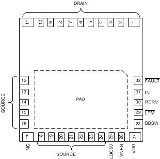
LMG3411R150 LMG3410R150 pin_diagram_snosd10.gif

Pin Functions

PIN I/O(1) DESCRIPTION
NAME NO.
BBSW 28 P Internal buck-boost converter switch pin. Connect an inductor from this point to source
DRAIN 1-11 P Power transistor drain
FAULT 32 O Fault output, push-pull, active low
IN 31 I CMOS-compatible non-inverting gate drive input; IN pin needs to be kept low at least 10 ns after the LDO 5 V is in regulation to reset the FAULT pin.
LDO5V 25 P 5-V LDO output for external digital isolator.
LPM 29 I Enables low-power-mode by connecting the pin to source
SOURCE 12-16, 18-24 P Power transistor source, die-attach pad, thermal sink, signal ground reference
RDRV 30 I Drive strength selection pin. Connect a resistor from this pin to ground to set the turn-on drive strength to control slew rate,
VDD 27 P 12-V power input, relative to source. Supplies 5-V rail and gate drive supply.
VNEG 26 P Negative supply output, bypass to source with 1-µF capacitor
NC 17 Not connected, connect to source or leave floating.
PAD P Thermal Pad, tie to source with multiple vias.
I = Input, O = Output, P = Power