SNOU177 December 2020 LM74700-Q1
4.1 PCB Drawings
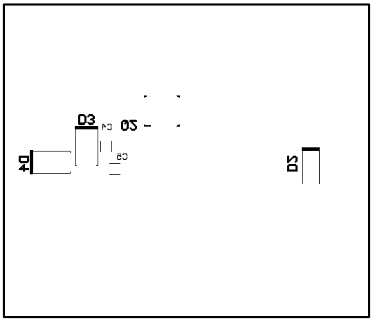
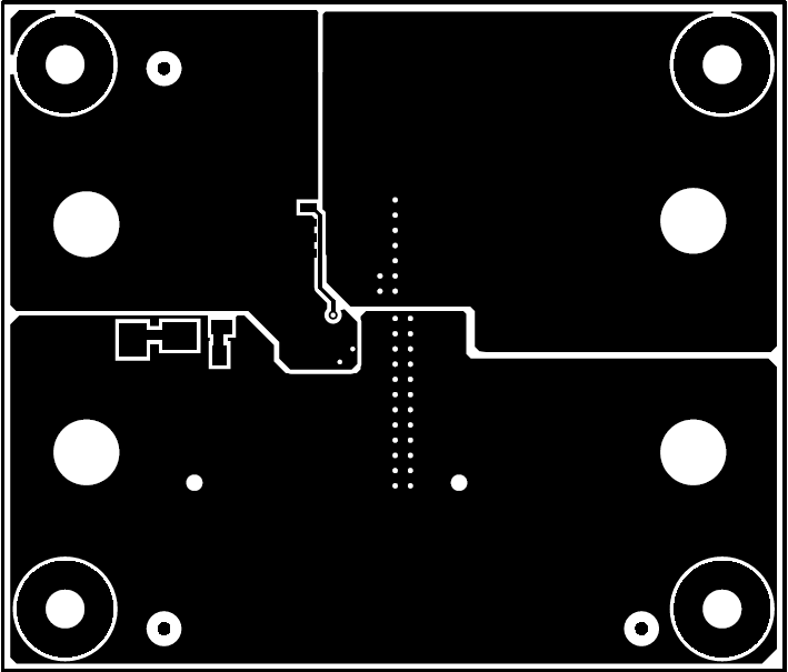
Figure 4-1 through Figure 4-4 show component placement and layout of this EVM.
 Figure 4-1 LM74700DDFEVM Top Side Placement
 Figure 4-2 LM74700DDFEVM Bottom Side Placement
 Figure 4-3 LM74700DDFEVM Top Layer Routing
 Figure 4-4 LM74700DDFEVM Bottom Layer Routing