SNOU206 October 2024 LMG2640
2.1.6 Heat Sink
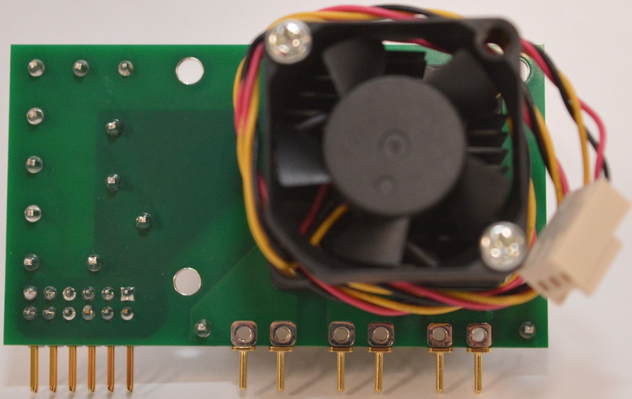
The heat sink is installed to help with heat dissipation of the LMG2640. Exposed copper pads are attached to the die attach pad (DAP) on the high-side and low-side devices to provide a low thermal impedance point for the heat sink. The two copper pads have a high-voltage potential difference between them, therefore an electrically isolated thermal interface material (TIM) is required.
For best thermal dissipation and board level reliability, recommendations for thermal via pattern and solder paste example are provided in the LMG2640 Integrated 650V GaN Half Bridge data sheet. Pin numbers 1, 13, 17, 21, 33, 37, and 40 are NC (no connection) which are used to anchor QFN package to PCB. These pins must be soldered to PCB landing pads which have to be non-solder mask defined pads and must not be physically connected to any other metal on the PCB. Internally, pins 1 and 13 are connected to DH and pins 17, 21, 37 are connected to AGND, SL, and PADL. Pin 40 needs to be connected to PADH. All pads must be NSMD for mechanical performance, refer to the device data sheet for trace connection recommendations to the pads. Filling the thermal pad with thermal vias is recommended for thermal performance. Fill and planarize vias.
In this daughter card design, S05MZZ3S-A heat sink and GR80B, thermal interface material has been used. More details on thermal performance and comparison between different TIM are shown in Thermal Performance of QFN 12x12 Package for 600V GaN Power Stage application note.
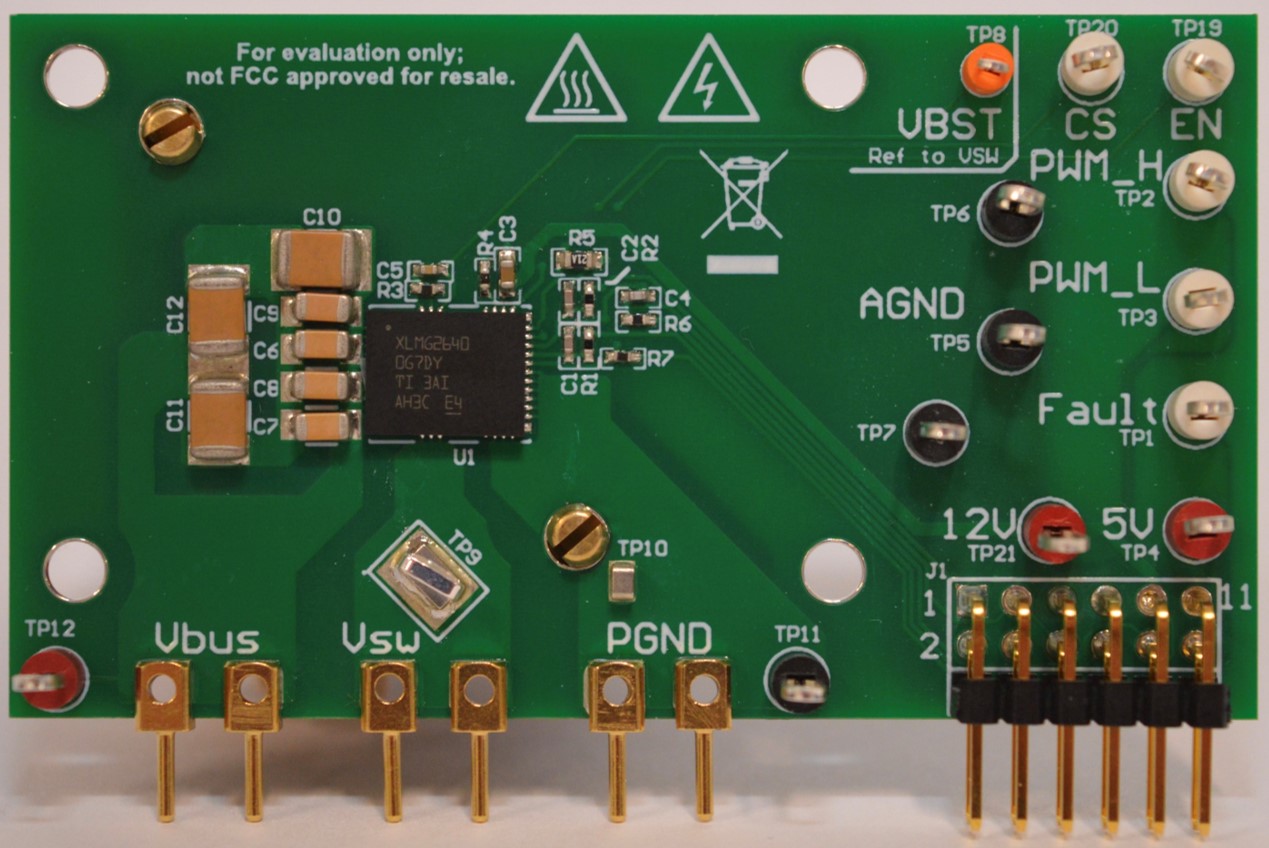
 Figure 2-1 EVM (Top View)
 Figure 2-2 EVM (Bottom View)