SNVA389B July 2009 – February 2022 LM3000
7 PCB Layout
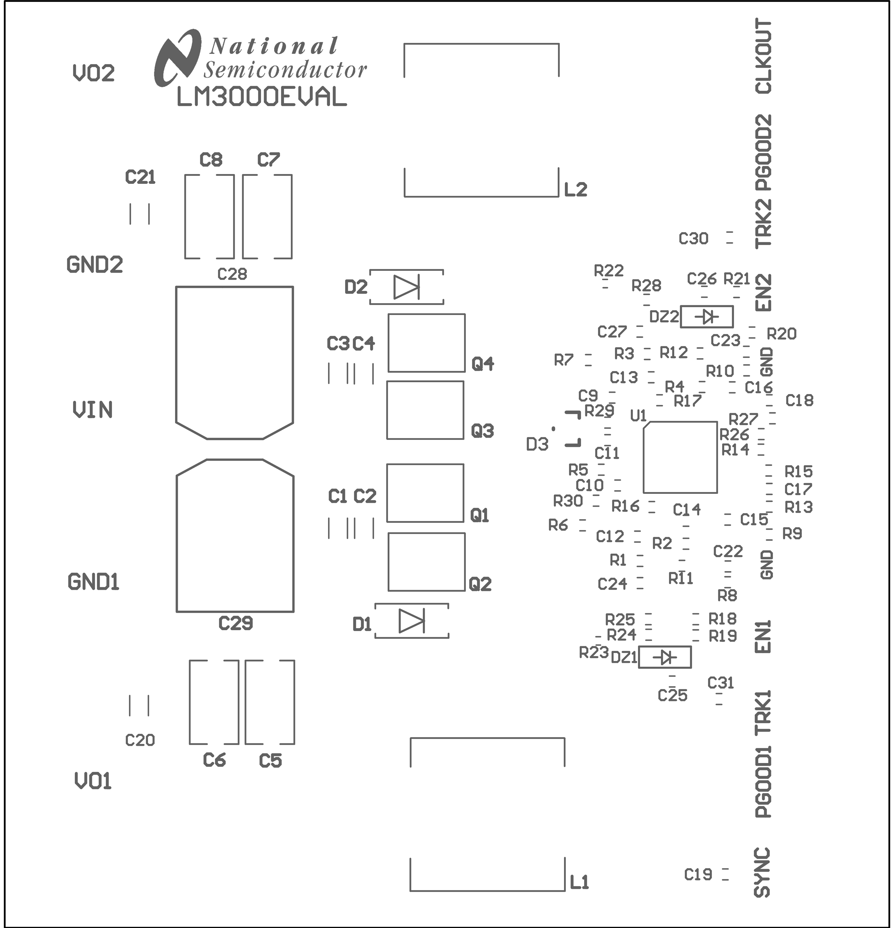 Figure 7-1 Top Overlay as Viewed from Top
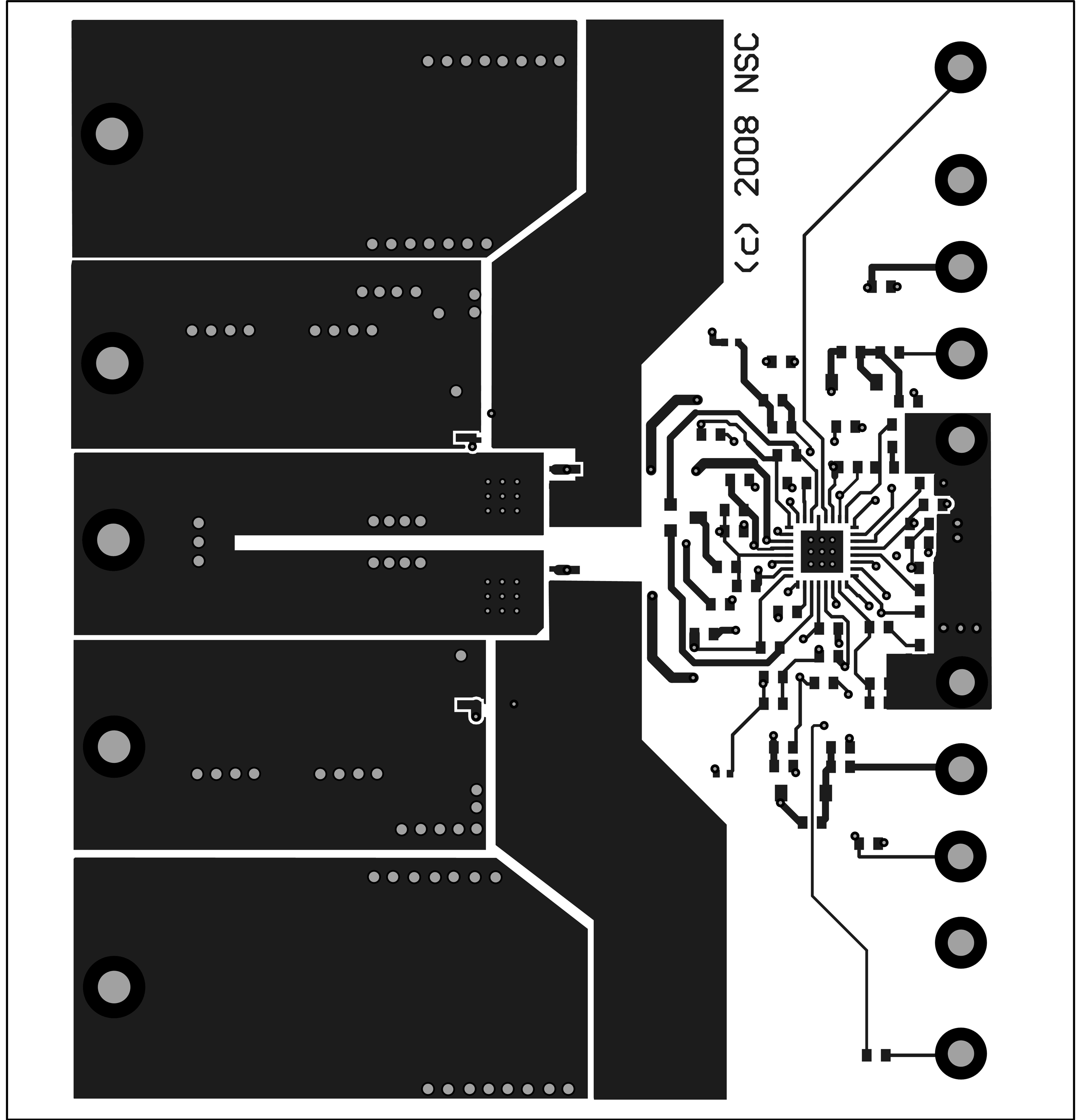 Figure 7-2 Top Layer as Viewed from Top
 Figure 7-3 Bottom Overlay as Viewed from Top
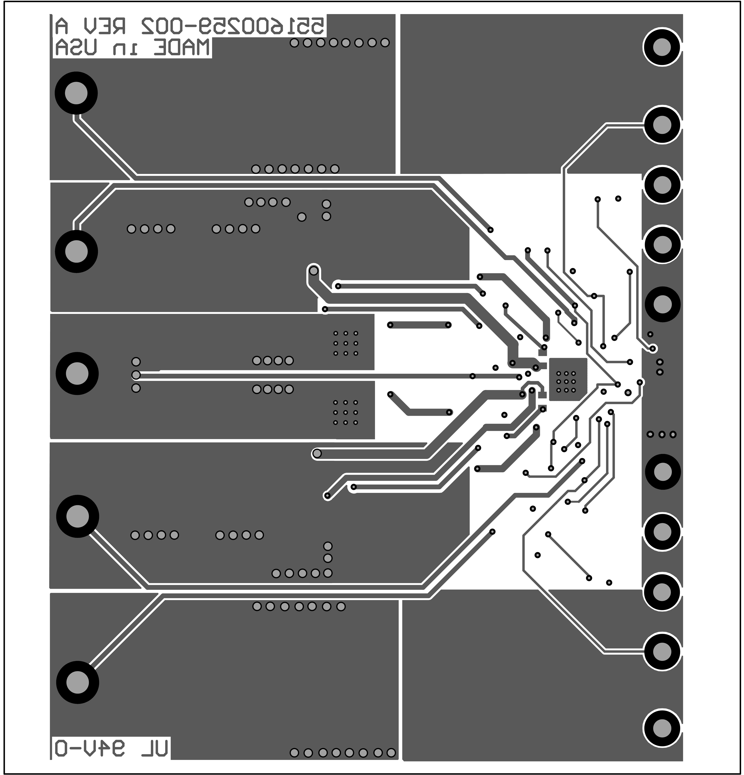 Figure 7-4 Bottom Layer as Viewed from Top
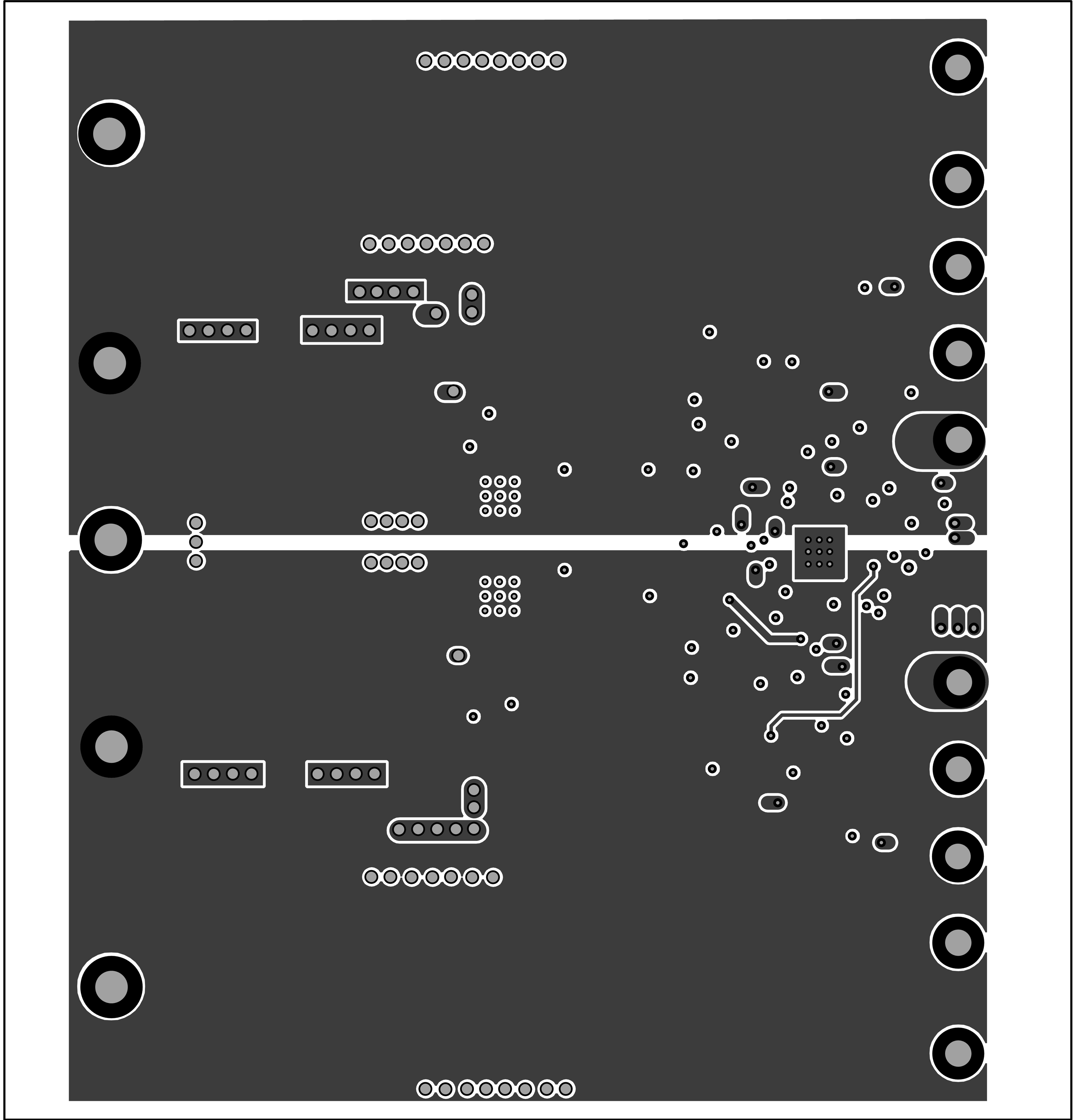 Figure 7-5 Internal Layer 1 as Viewed from Top
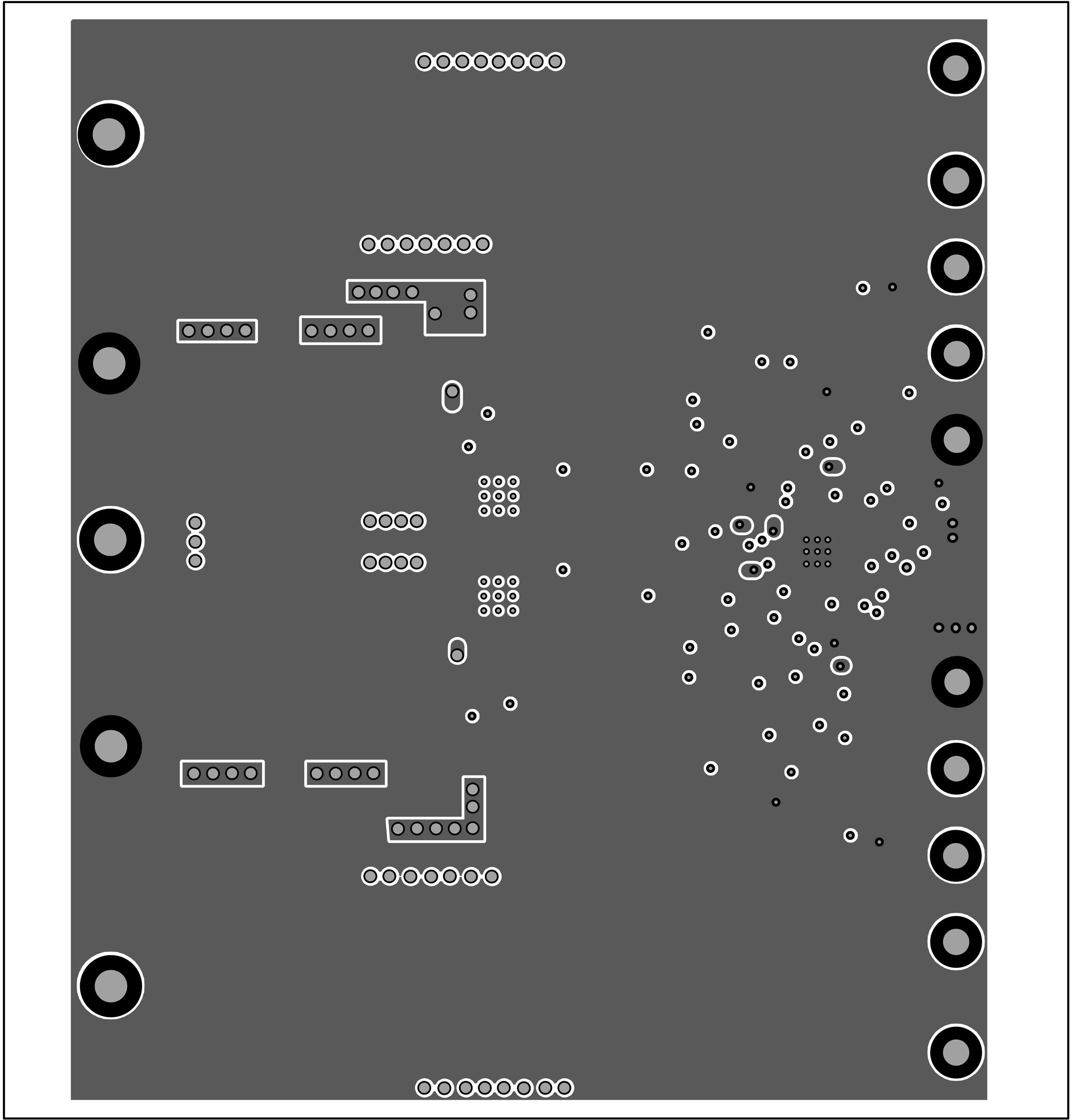 Figure 7-6 Internal Layer 2 as Viewed from Top