SNVA484B October 2011 – March 2024 LM5113
5.2 PCB Layouts
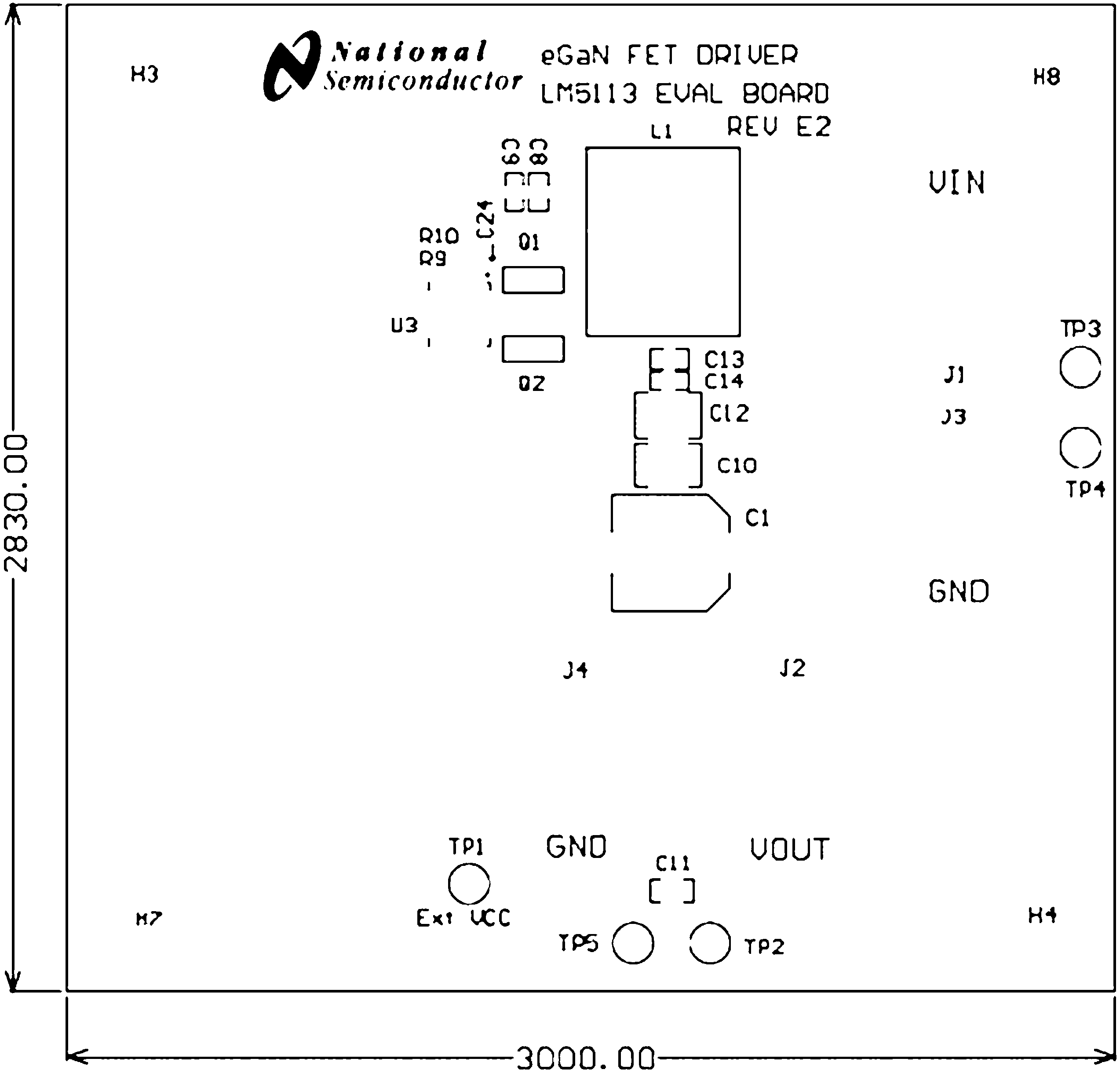 Figure 5-2 Top Side Silk Screen
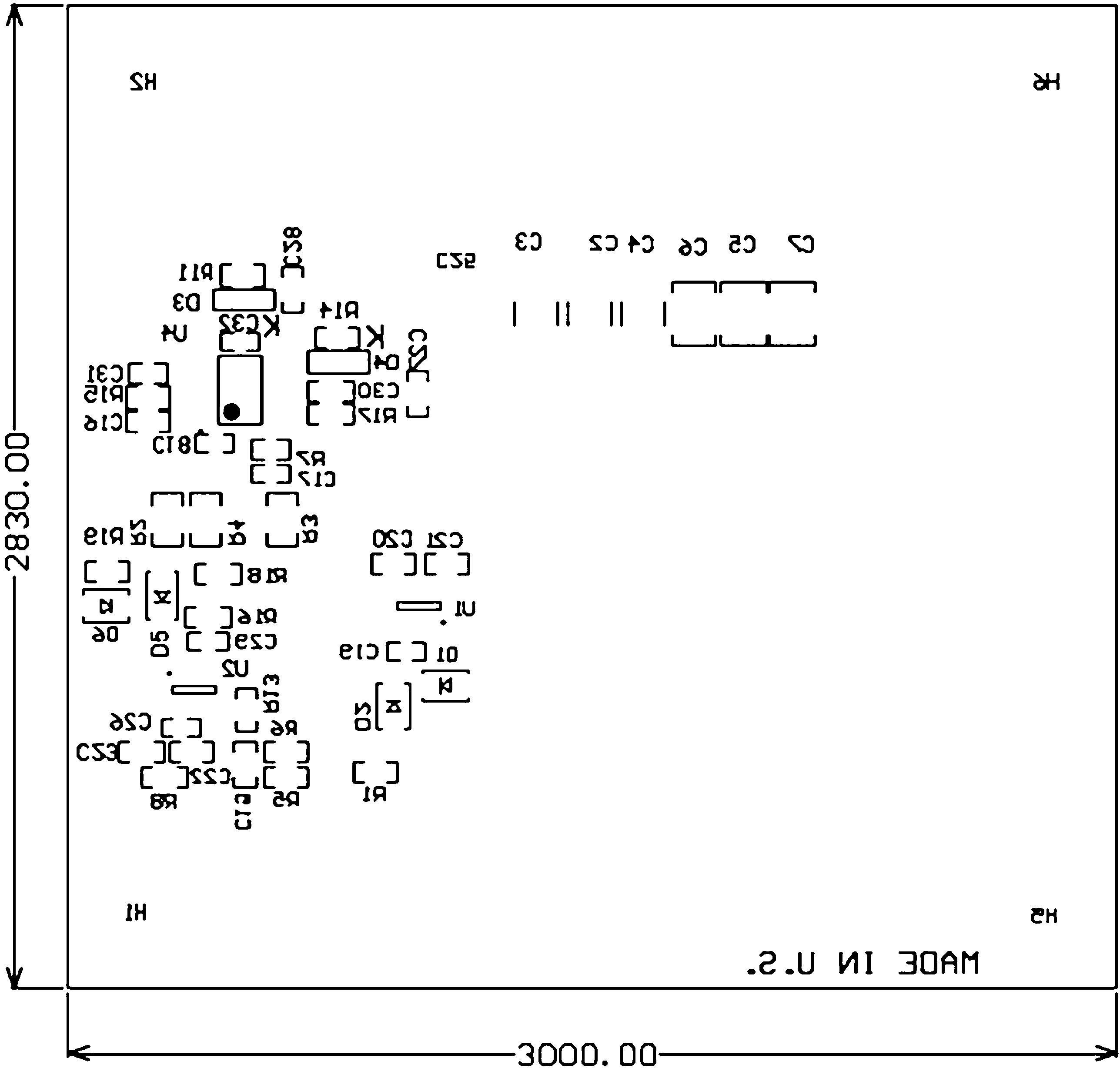 Figure 5-3 Bottom Side Silk Screen
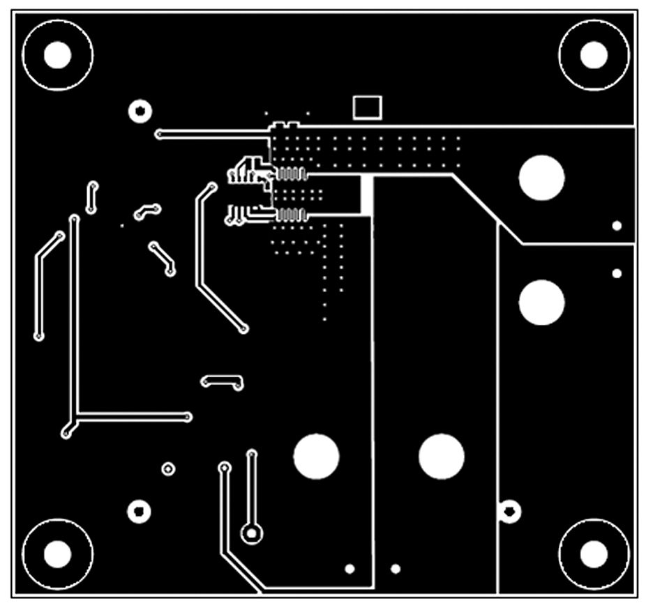 Figure 5-4 Top Layer
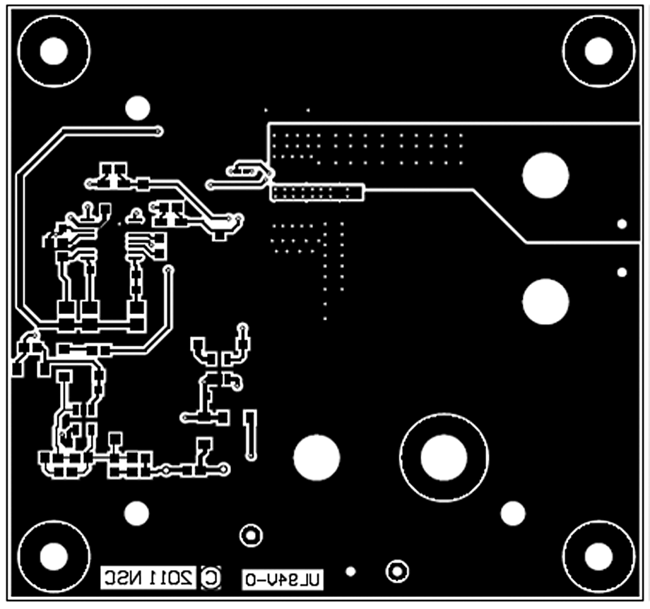 Figure 5-5 Bottom Layer
SNVA484B October 2011 – March 2024 LM5113
 Figure 5-2 Top Side Silk Screen
 Figure 5-3 Bottom Side Silk Screen
 Figure 5-4 Top Layer
 Figure 5-5 Bottom Layer