SNVS536F October 2007 – July 2015 LM2757
PRODUCTION DATA.
- 1 Features
- 2 Applications
- 3 Description
- 4 Revision History
- 5 Device Options
- 6 Pin Configuration and Functions
- 7 Specifications
- 8 Detailed Description
- 9 Application and Implementation
- 10Power Supply Recommendations
- 11Layout
- 12Device and Documentation Support
- 13Mechanical, Packaging, and Orderable Information
9 Application and Implementation
NOTE
Information in the following applications sections is not part of the TI component specification, and TI does not warrant its accuracy or completeness. TI’s customers are responsible for determining suitability of components for their purposes. Customers should validate and test their design implementation to confirm system functionality.
9.1 Application Information
The LM2757 can create a 4.1-V, 4.5-V or 5-V system rail capable of delivering up to 180 mA of output current to the load. The 1.242-MHz switched capacitor boost allows for the use of small value discrete external components.
9.2 Typical Application
9.2.1 Switched-Capacitor Boost Regulator
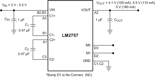 Figure 21. LM2757 Typical Application
9.2.1.1 Design Requirements
Example requirements for typical switched-capacitor boost regulator applications:
Table 2. Design Parameters
| DESIGN PARAMETER | EXAMPLE VALUE |
|---|---|
| Input voltage range | 2.7 V to 5.5 V |
| Output current | 0 to 180 mA |
| Boost switching frequency | 1.242 MHz |
9.2.1.2 Detailed Design Procedure
9.2.1.2.1 Recommended Capacitor Types
The LM2757 requires 4 external capacitors for proper operation. Surface-mount multi-layer ceramic capacitors are recommended. These capacitors are small, inexpensive and have very low equivalent series resistance (ESR, ≤ 15 mΩ typical). Tantalum capacitors, OS-CON capacitors, and aluminum electrolytic capacitors generally are not recommended for use with the LM2757 due to their high ESR, as compared to ceramic capacitors.
For most applications, ceramic capacitors with an X7R or X5R temperature characteristic are preferred for use with the LM2757. These capacitors have tight capacitance tolerance (as good as ±10%) and hold their value over temperature (X7R: ±15% over –55°C to 125°C; X5R: ±15% over –55°C to 85°C).
Capacitors with a Y5V or Z5U temperature characteristic are generally not recommended for use with the LM2757. These types of capacitors typically have wide capacitance tolerance (80%, –20%) and vary significantly over temperature (Y5V: +22%, –82% over –30°C to +85°C range; Z5U: 22%, –56% over a 10°C to 85°C range). Under some conditions, a 1-µF-rated Y5V or Z5U capacitor could have a capacitance as low as 0.1 µF. Such detrimental deviation is likely to cause Y5V and Z5U capacitors to fail to meet the minimum capacitance requirements of the LM2757.
Net capacitance of a ceramic capacitor decreases with increased DC bias. This degradation can result in lower capacitance than expected on the input and/or output, resulting in higher ripple voltages and currents. Using capacitors at DC bias voltages significantly below the capacitor voltage rating usually minimizes DC bias effects. Consult capacitor manufacturers for information on capacitor DC bias characteristics.
Capacitance characteristics can vary quite dramatically with different application conditions, capacitor types, and capacitor manufacturers. It is strongly recommended that the LM2757 circuit be thoroughly evaluated early in the design-in process with the mass-production capacitors of choice. This helps ensure that any such variability in capacitance does not negatively impact circuit performance.
The voltage rating of the output capacitor should be 10 V or more. For example, a 10-V 0603 1-µF capacitor is acceptable for use with the LM2757, as long as the capacitance does not fall below a minimum of 0.5 µF in the intended application. All other capacitors should have a voltage rating at or above the maximum input voltage of the application. The capacitors should be selected such that the capacitance on the input does not fall below 0.7 µF, and the capacitance of the flying capacitors does not fall below 0.2 µF.
Table 3 lists some leading ceramic capacitor manufacturers.
Table 3. Manufacturers of Suggested Capacitors
| MANUFACTURER | CONTACT INFORMATION |
|---|---|
| AVX | www.avx.com |
| Murata | www.murata.com |
| Taiyo-Yuden | www.t-yuden.com |
| TDK | www.component.tdk.com |
| Vishay-Vitramon | www.vishay.com |
9.2.1.2.2 Output Capacitor And Output Voltage Ripple
The output capacitor in the LM2757 circuit (COUT) directly impacts the magnitude of output voltage ripple. Other prominent factors also affecting output voltage ripple include input voltage, output current, and flying capacitance. Due to the complexity of the regulation topology, providing equations or models to approximate the magnitude of the ripple can not be easily accomplished. But one important generalization can be made: increasing (decreasing) the output capacitance results in a proportional decrease (increase) in output voltage ripple.
In typical high-current applications, a 1-µF low-ESR ceramic output capacitor is recommended. Different output capacitance values can be used to reduce ripple, shrink the solution size, and/or cut the cost of the solution. But changing the output capacitor may also require changing the flying capacitor and/or input capacitor to maintain good overall circuit performance. Performance of the LM2757 with different capacitor setups in discussed in Recommended Capacitance.
High ESR in the output capacitor increases output voltage ripple. If a ceramic capacitor is used at the output, this is usually not a concern because the ESR of a ceramic capacitor is typically very low and has only a minimal impact on ripple magnitudes. If a different capacitor type with higher ESR is used (tantalum, for example), the ESR could result in high ripple. To eliminate this effect, the net output ESR can be significantly reduced by placing a low-ESR ceramic capacitor in parallel with the primary output capacitor. The low ESR of the ceramic capacitor is in parallel with the higher ESR, resulting in a low net ESR based on the principles of parallel resistance reduction.
9.2.1.2.3 Input Capacitor And Input Voltage Ripple
The input capacitor (CIN) is a reservoir of charge that aids a quick transfer of charge from the supply to the flying capacitors during the charge phase of operation. The input capacitor helps to keep the input voltage from drooping at the start of the charge phase when the flying capacitors are connected to the input. It also filters noise on the input pin, keeping this noise out of sensitive internal analog circuitry that is biased off the input line.
Much like the relationship between the output capacitance and output voltage ripple, input capacitance has a dominant and first-order effect on input ripple magnitude. Increasing (decreasing) the input capacitance results in a proportional decrease (increase) in input voltage ripple. Input voltage, output current, and flying capacitance also affects input ripple levels to some degree.
In typical high-current applications, a 1-µF low-ESR ceramic capacitor is recommended on the input. Different input capacitance values can be used to reduce ripple, shrink the solution size, and/or cut the cost of the solution. But changing the input capacitor may also require changing the flying capacitor and/or output capacitor to maintain good overall circuit performance. Performance of the LM2757 with different capacitor setups is discussed in Recommended Capacitance.
9.2.1.2.4 Flying Capacitors
The flying capacitors (C1, C2) transfer charge from the input to the output. Flying capacitance can impact both output current capability and ripple magnitudes. If flying capacitance is too small, the LM2757 may not be able to regulate the output voltage when load currents are high. On the other hand, if the flying capacitance is too large, the flying capacitor might overwhelm the input and output capacitors, resulting in increased input and output ripple.
In typical high-current applications, 0.47-µF low-ESR ceramic capacitors are recommended for the flying capacitors. Polarized capacitors (tantalum, aluminum electrolytic, etc.) must not be used for the flying capacitor, as they could become reverse-biased during LM2757 operation.
9.2.1.2.5 Recommended Capacitance
The data in Table 4 can be used to assist in the selection of capacitance for each node that best balances solution size and cost with the electrical requirements of the application.
As previously discussed, input and output ripple voltages varies with output current and input voltage. The numbers provided show expected ripple voltage with VIN = 3.6 V and a load current of 200 mA at 5-V output, 100 mA at 4.5-V output, and 100 mA at 4.1-V output. Table 4 offers a first look at approximate ripple levels and provides a comparison of different capacitance configurations, but is not intended to ensure performance. With any capacitance configuration chosen, always verify that the performance of the ripple waveforms are suitable for the intended application. The same capacitance value must be used for all the flying capacitors. For output regulation performance with different capacitor configurations, please refer to the output voltage vs. input voltage graphs in Typical Characteristics. The output voltage regulation is typically better when using capacitors with a higher capacitance value and a higher voltage bias rating than the nominal voltage applied to them, as can be seen in the graphs, but this may have an impact in capacitor case size. For typical high-current small solution size applications, 1-µF capacitance X5R temperature characteristic rating 0402 (C1005) case size and 10-V bias or higher capacitors can be used for the input, output and flying capacitors. According to current capacitor offerings, there are no capacitors in the 0201 (C0603) case size that satisfy the minimum capacitance requirements of the LM2757 circuit. When selecting capacitors, those with the highest voltage bias rating available from the capacitor supplier are preferred.
Table 4. LM2757 Performance With Different Capacitor Configurations(1)
| CAPACITOR CONFIGURATION (VIN = 3.6 V) |
5-V, 200-mA OUTPUT RIPPLE (mV)(typical) | 4.5-V, 100-mA OUTPUT RIPPLE (mV) (typical) | 4.1-V, 100-mA OUTPUT RIPPLE (mV)(typical) |
|---|---|---|---|
| CIN = 1 µF, COUT = 1 µF, C1 and C2 = 0.47 µF | 32 | 12 | 11 |
| CIN = 0.68 µF, COUT = 1 µF, C1 and C2 = 0.47 µF | 32 | 11 | 11 |
| CIN = 0.68 µF, COUT = 0.47 µF, C1 and C2 = 0.47 µF | 51 | 151 | 15 |
| CIN = 0.68 µF, COUT = 0.47 µF, C1 and C2 = 0.22 µF | 53 | 181 | 18 |
9.2.1.3 Application Curves
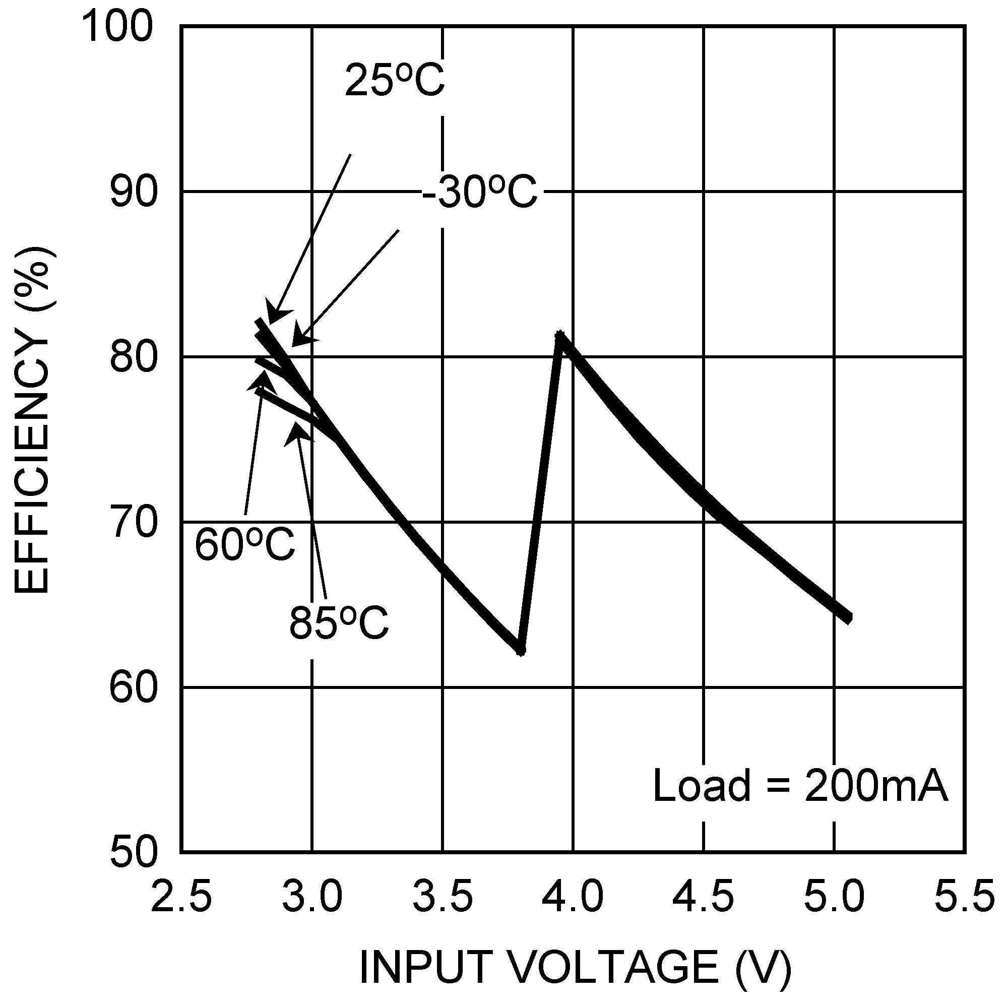
| 5-V Mode |
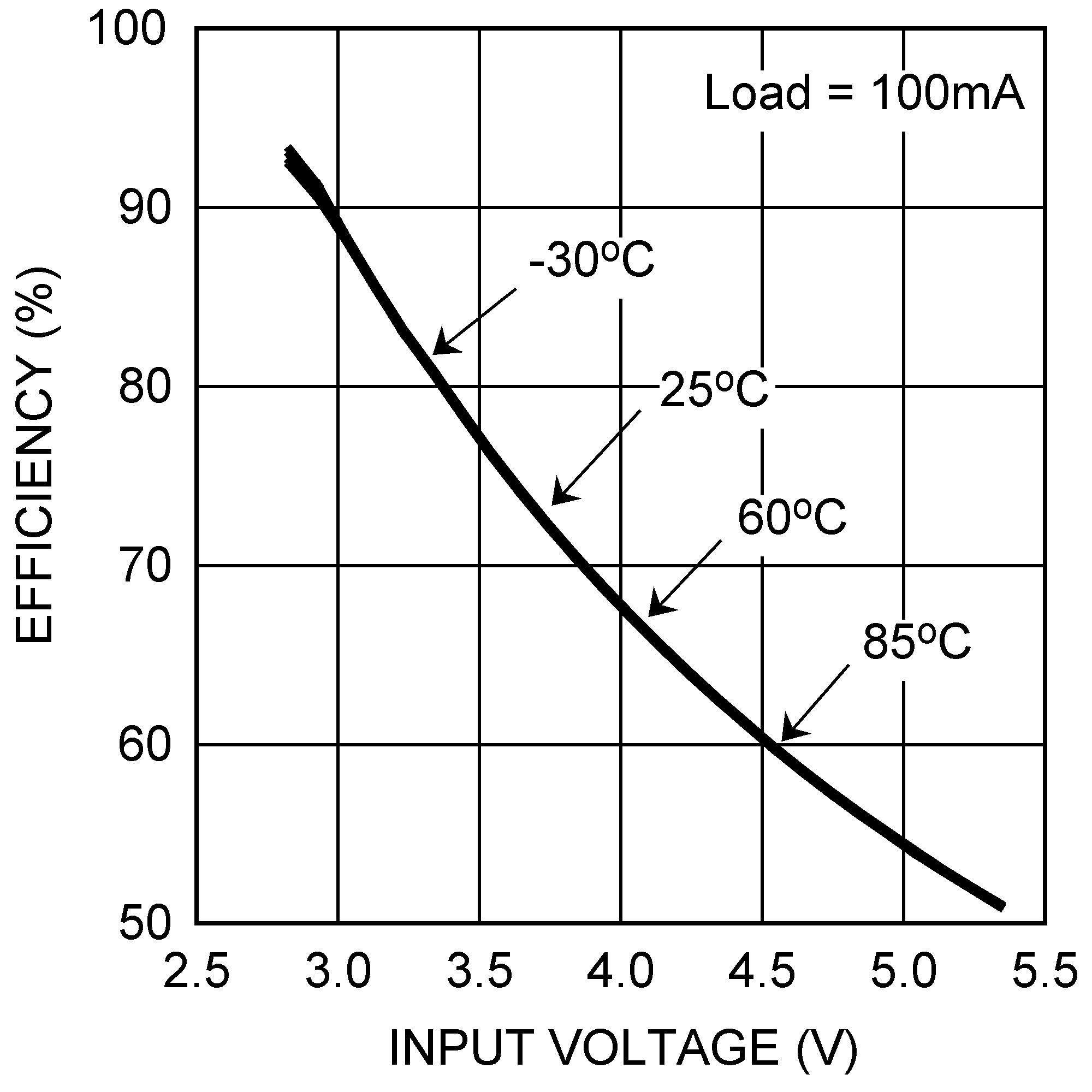
| 4.1-V Mode |
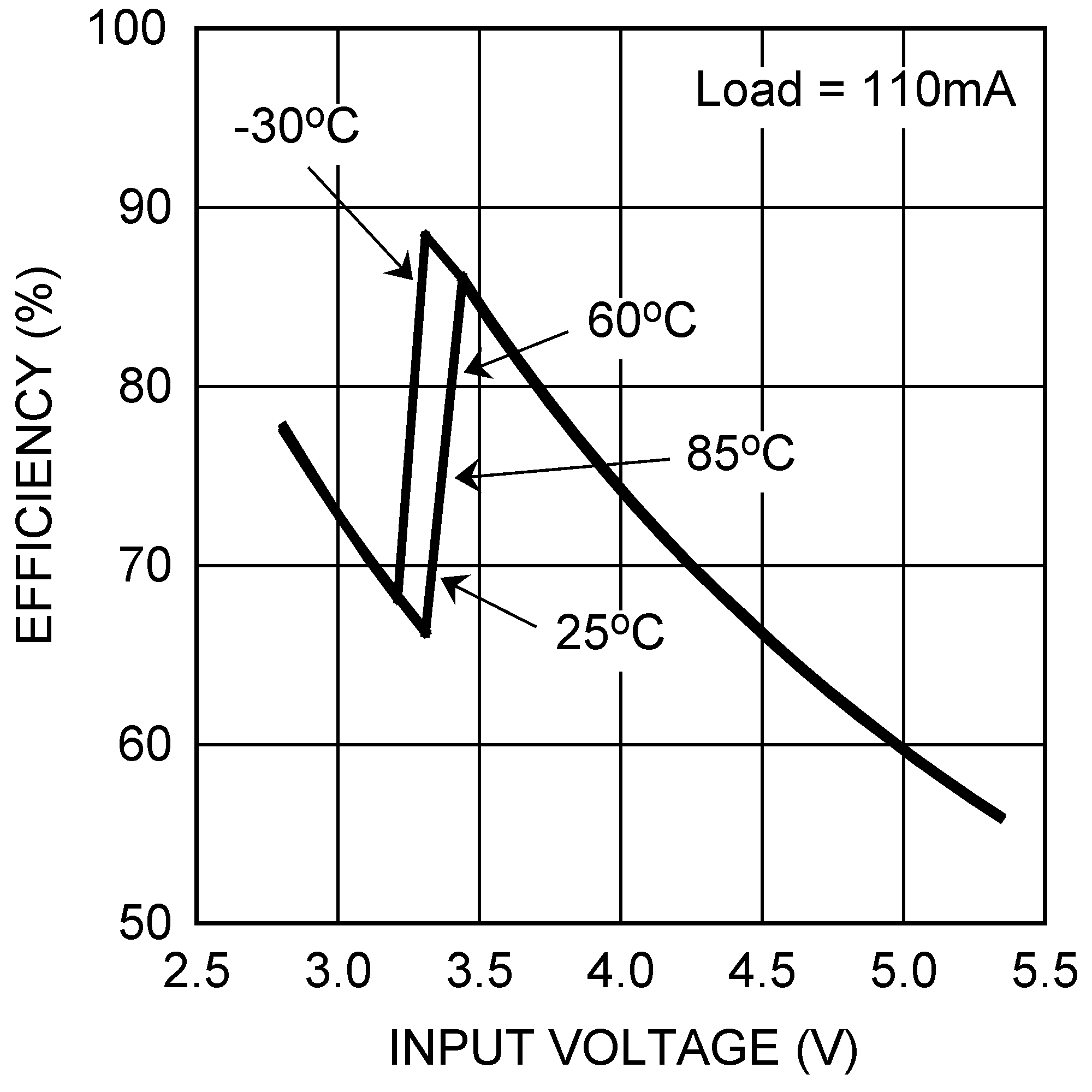
| 4.5-V Mode |
9.2.2 USB OTG / Mobile HDMI Power Supply
The 5-V output mode is normally used for the USB OTG / Mobile HDMI application. Therefore, the LM2757 can be enabled or disabled by applying a logic signal on only the M1 pin while grounding the M0 pin. Depending on the USB/HDMI mode of the application, the LM2757 can be enabled to drive the power bus line (Host), or disabled to put its output in high impedance allowing an external supply to drive the bus line (Slave). In addition to the high-impedance backdrive protection, the output current limit protection is 250 mA (typical), well within the USB OTG and HDMI requirements.
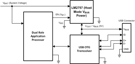 Figure 25. USB OTG / Mobile HDMI
9.2.3 Supercapacitor Flash Driver
Using the 5-V output voltage mode, the LM2757 can charge a supercapacitor for LED flash applications while limiting the peak current drawn off the battery during the charge cycle. The LM2757 can be disabled for the Flash event, placing its output in high impedance with the input. In this way, all charge for the flash LED(s) comes directly off the supercapacitor and does not load the main battery line. The LM2757 can be enabled or disabled by applying a logic signal on only the M1 pin while grounding the M0 pin.
Special consideration must be given when using supercapacitors for LED flash applications where the voltage on the capacitor is charged to a fixed value. This is due to the possible power management issues that can arise as a result of the high flash current and wide tolerance ranges (V–I characteristics) of typical flash LEDs. If the voltage across the Flash LED(s) is not managed, damage may occur where a relatively low Vf LED is overdriven or places excessive voltage across the bottom control FET. To help avoid this issue, the use of a high-power current sink is advised in applications where the forward voltage specification of the flash LED has a wide range.
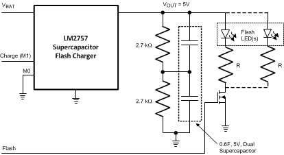 Figure 26. Supercapacitor Flash Driver
9.2.4 LED Driver
The 5-V, 4.5-V, or the 4.1-V mode can be used depending on the forward voltage and load requirements of the LED application. The LM2757 can be enabled or disabled by applying the appropriate combination of logic signals on the M1 and M0 pins. LED current for each string in this application is limited by the voltage across the string's ballast resistor, which is dependent on the output voltage mode selected and the V-I profile of each LED used.
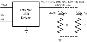 Figure 27. LED Driver