SNVS536F October 2007 – July 2015 LM2757
PRODUCTION DATA.
- 1 Features
- 2 Applications
- 3 Description
- 4 Revision History
- 5 Device Options
- 6 Pin Configuration and Functions
- 7 Specifications
- 8 Detailed Description
- 9 Application and Implementation
- 10Power Supply Recommendations
- 11Layout
- 12Device and Documentation Support
- 13Mechanical, Packaging, and Orderable Information
7 Specifications
7.1 Absolute Maximum Ratings
over operating free-air temperature range (unless otherwise noted)(1)(2)(3)| MIN | MAX | UNIT | ||
|---|---|---|---|---|
| VIN pin: voltage to GND | –0.3 | 6 | V | |
| M0, M1 pins: voltage to GND | –0.3 | 6 | V | |
| Continuous power dissipation(4)
|
Internally Limited | |||
| Junction temperature, TJ-MAX | 150 | °C | ||
| Maximum lead temperature (soldering, 10 sec.) | 265 | °C | ||
| Storage temperature, Tstg | –65 | 150 | °C | |
(1) Stresses beyond those listed under Absolute Maximum Ratings may cause permanent damage to the device. These are stress ratings only, which do not imply functional operation of the device at these or any other conditions beyond those indicated under Recommended Operating Conditions. Exposure to absolute-maximum-rated conditions for extended periods may affect device reliability.
(2) If Military/Aerospace specified devices are required, please contact the TI Sales Office/ Distributors for availability and specifications.
(3) All voltages are with respect to the potential at the GND pins.
(4) Internal thermal shutdown circuitry protects the device from permanent damage. Thermal shutdown engages at TJ = 145°C (typical) and disengages at TJ = 135°C (typical).
7.2 ESD Ratings
| VALUE | UNIT | |||
|---|---|---|---|---|
| V(ESD) | Electrostatic discharge | Human-body model (HBM), per ANSI/ESDA/JEDEC JS-001(1) | ±2500 | V |
(1) JEDEC document JEP155 states that 500-V HBM allows safe manufacturing with a standard ESD control process.
7.3 Recommended Operating Conditions
over operating free-air temperature range (unless otherwise noted)(1)(3)| MIN | NOM | MAX | UNIT | ||
|---|---|---|---|---|---|
| Input voltage | 2.7 | 5.5 | °C | ||
| Junction temperature, TJ | –30 | 110 | °C | ||
| Ambient temperature, TA(2) | –30 | 85 | °C | ||
(1) Stresses beyond those listed under Absolute Maximum Ratings may cause permanent damage to the device. These are stress ratings only, which do not imply functional operation of the device at these or any other conditions beyond those indicated under Recommended Operating Conditions. Exposure to absolute-maximum-rated conditions for extended periods may affect device reliability.
(2) In applications where high power dissipation and/or poor package thermal resistance is present, the maximum ambient temperature may have to be derated. Maximum ambient temperature (TA-MAX) is dependent on the maximum operating junction temperature (TJMAX-OP = 125°C), the maximum power dissipation of the device in the application (PD-MAX), and the junction-to-ambient thermal resistance of the part/package in the application (RθJA), as given by the following equation: TA-MAX = TJ-MAX-OP – (RθJA × PD-MAX).
7.4 Thermal Information
| THERMAL METRIC(1) | LM2757 | UNIT | |
|---|---|---|---|
| YFQ (DSBGA) | |||
| 12 PINS | |||
| RθJA | Junction-to-ambient thermal resistance | 75 | °C/W |
(1) For more information about traditional and new thermal metrics, see the Semiconductor and IC Package Thermal Metrics application report, SPRA953.
7.5 Electrical Characteristics
Unless otherwise specified, typical (TYP) limits in apply for TA = 25ºC; minimium (MIN) and maximum (MAX) limits apply over the full operating ambient temperature range (–30°C ≤ TA ≤ +85°C) . Unless otherwise noted, specifications apply to Typical Application with: VIN = 3.6 V, V(M0) = 0 V, V(M1) = VIN, CIN = C2 = 0.47 µF, CIN= COUT = 1 µF.(1)(2)(3)| PARAMETER | TEST CONDITIONS | MIN | TYP | MAX | UNIT | |
|---|---|---|---|---|---|---|
| VOUT | Output voltage | 3.2 V ≤ VIN ≤ 5.5 V –30°C ≤ TA ≤ +60°C IOUT = 0 to 180 mA V(M0) = 0V, V(M1) = VIN |
4.870 (−2.6%) |
5 | 5.130 (2.6%) |
V |
| 3. V ≤ VIN ≤ 5.5 V –30°C ≤ TA ≤ +85°C IOUT = 0 to 150 mA V(M0) = 0V, V(M1) = VIN |
4.865 (−2.7%) |
5 | 5.130 (2.6%) |
|||
| 3 V ≤ VIN ≤ 5.5 V IOUT = 0 to 110 mA V(M0) = VIN, V(M1) = 0 V |
4.406 (–2.1%) |
4.5 | 4.613 (2.5%) |
|||
| 3. V ≤ VIN ≤ 5.5 V IOUT = 0 to 100 mA V(M0) = VIN, V(M1) = VIN |
3.985 (–2.8%) |
4.1 | 4.223 (3%) |
|||
| IQ | Quiescent supply current | V(M0) = 0 V, V(M1) = VIN (5 V) IOUT = 0 mA VIN = 3.6 V |
2.4 | 2.79 | mA | |
| V(M0) = VIN, V(M1) = 0 V (4.5 V) IOUT = 0 mA VIN = 3.6 V |
1.5 | 1.80 | ||||
| V(M0) = VIN, V(M1) = VIN (4.1 V) IOUT = 0 mA VIN = 3.6 V |
1.3 | 1.65 | ||||
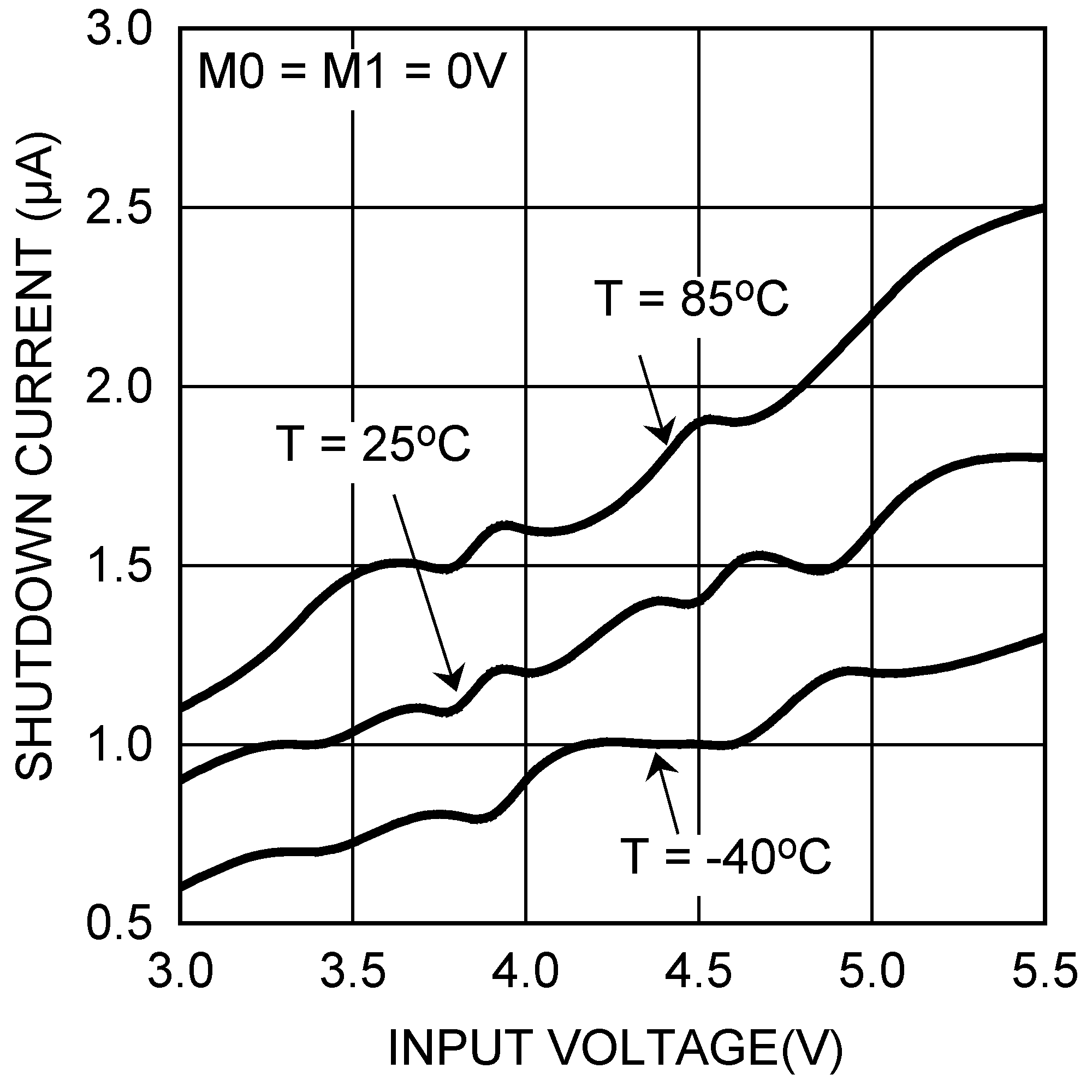
| ISD | Shutdown supply current | V(M0) = 0 V, V(M1) = 0 V VIN = 3.6 V |
1.1 | 2 | µA | |
| VR | Output ivoltage rpple | IOUT = 150 mA V(M0) = 0V, V(M1) = VIN (5 V) 3 V ≤ VIN ≤ 5.5 V |
20 | mVp–p | ||
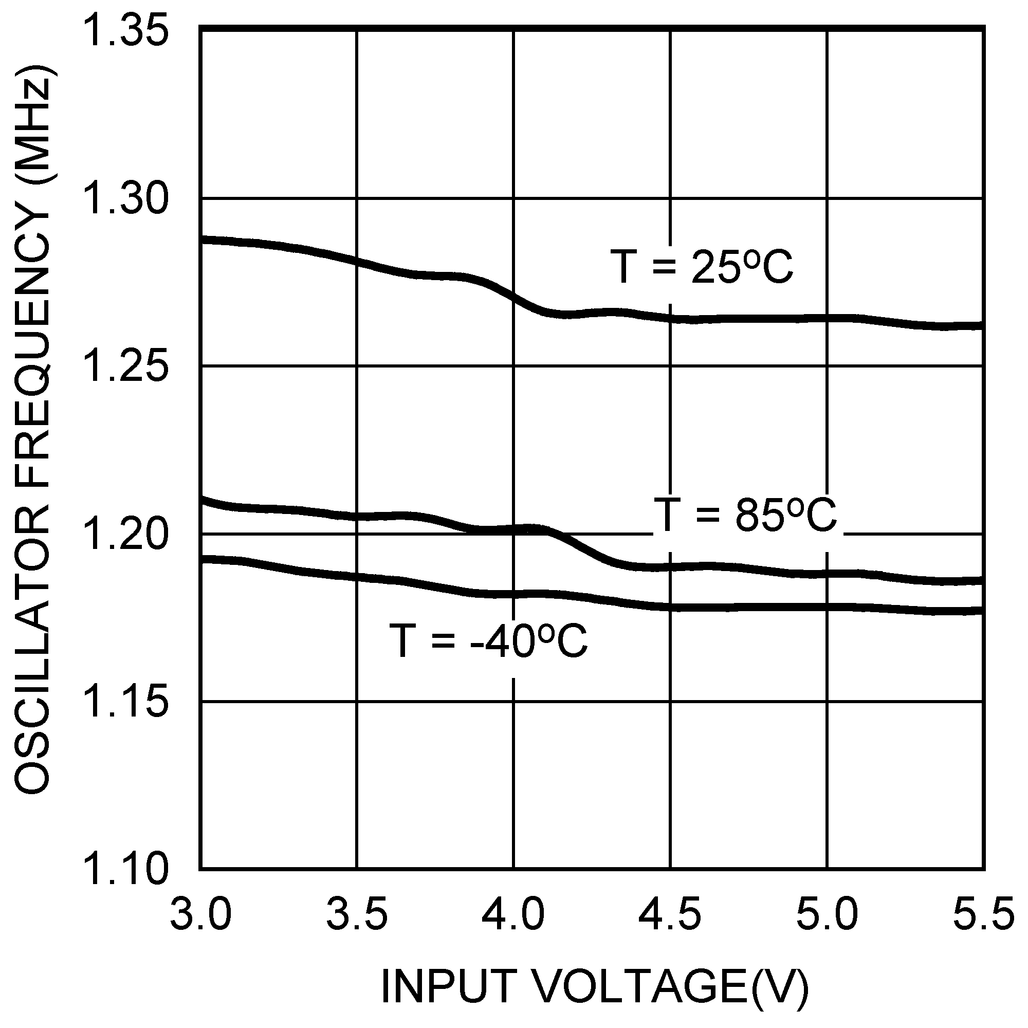
| ƒSW | Switching frequency | 3 V ≤ VIN ≤ 5.5 V | 0.932 (–25%) | 1.242 | 1.552 (+25%) | MHz |
| VIN | Logic input high | Input pins: M1, M0 3 V ≤ VIN ≤ 5.5 V |
1 | VIN | V | |
| VIL | Logic input low | Input pins: M1, M0 3 V ≤ VIN ≤ 5.5 V |
0 | 0.40 | V | |
| RPULLDOWN | Logic input pulldown resistance (M0, M1) |
V(M1, M0) = 5.5 V | 324 | 457 | kΩ | |
| IIH | Logic input high current | Input Pins: M1, M0 V(M1, M0) = 1.8 V(5) |
5 | µA | ||
| IIL | Logic input low current | Input Pins: M1, M0 V(M1, M0) = 0 V |
10 | nA | ||
| VG | Gain transition voltage | 1.5× to 2×, V(M0) = VIN, V(M1) = 0 V | 3.333 | V | ||
| 2× to 1.5×, V(M0) = VIN, V(M1) = 0 V | 3.413 | V | ||||
| Hysteresis, V(M0) = VIN, V(M1) = 0 V | 80 | mV | ||||
| 1.5× to 2×, V(M0) = 0 V, V(M1) = VIN | 3.87 | V | ||||
| 2× to 1.5×, V(M0) = 0 V, V(M1) = VIN | 3.93 | V | ||||
| Hysteresis, V(M0) = 0 V, V(M1) = VIN | 60 | mV | ||||
| ISC | Short-circuit output current | VOUT = 0 V | 250 | mA | ||
| ION | VOUT turnon time from shutdown (4) | 300 | µs | |||
(1) All voltages are with respect to the potential at the GND pins.
(2) Minimum and maximum limits are specified by design, test, or statistical analysis. Typical numbers are not ensured, but do represent the most likely norm.
(3) CIN, COUT, C1, C2: Low-ESR Surface-Mount Ceramic Capacitors (MLCCs) used in setting electrical characteristics.
(4) Turnon time is measured from when the M0 or M1 signal is pulled high until the output voltage crosses 90% of its final value.
(5) There is a 450-kΩ (typical) pulldown resistor connected internally to each logic input.
7.6 Typical Characteristics
Unless otherwise specified: VIN = 3.6 V, V(M0) = 0 V, V(M1) = VIN, C1 = C2 = 0.47 µF, CIN = COUT = 1 µF, TA = 25°C. Capacitors are low-ESR multi-layer ceramic capacitors (MLCC's).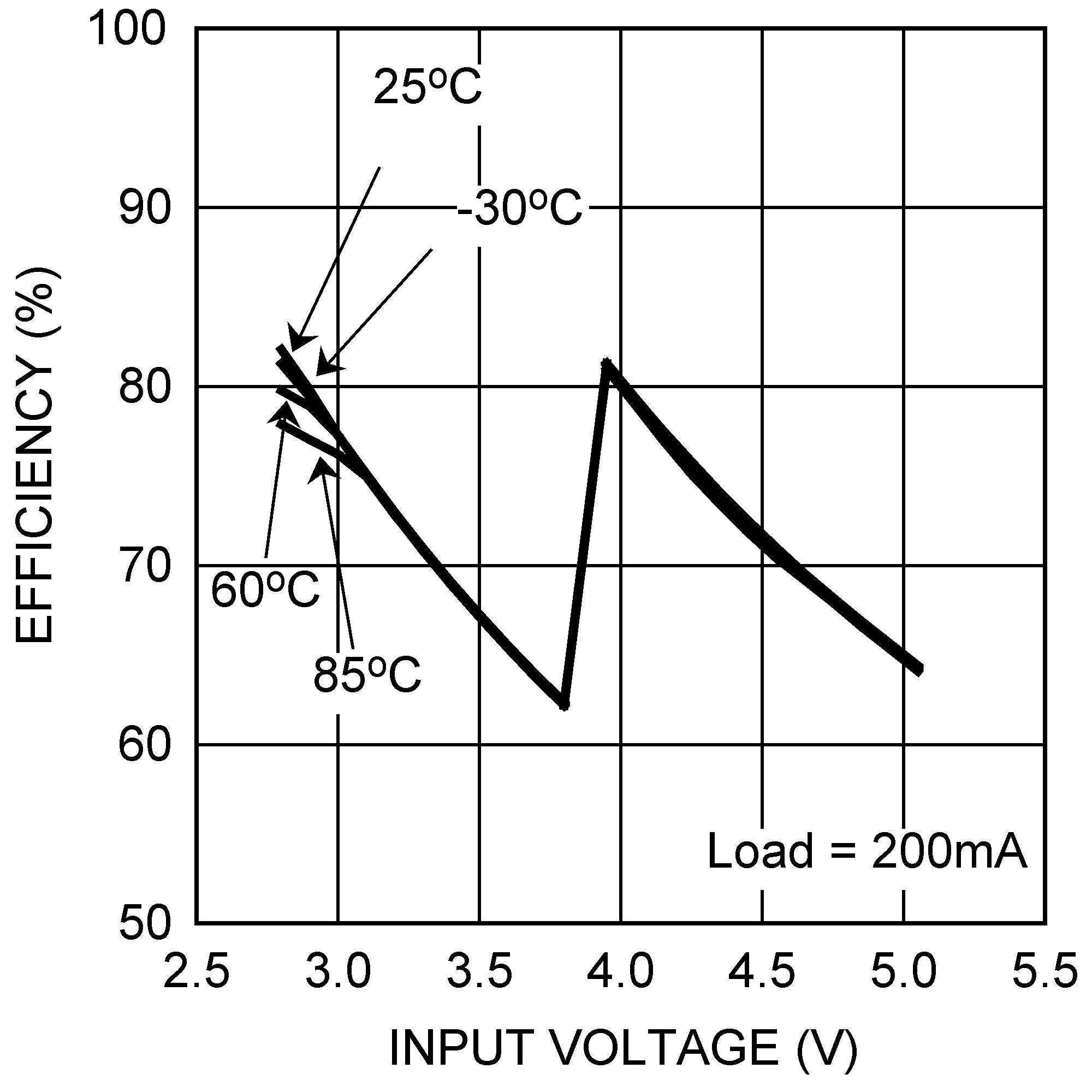
| 5-V Mode | ||
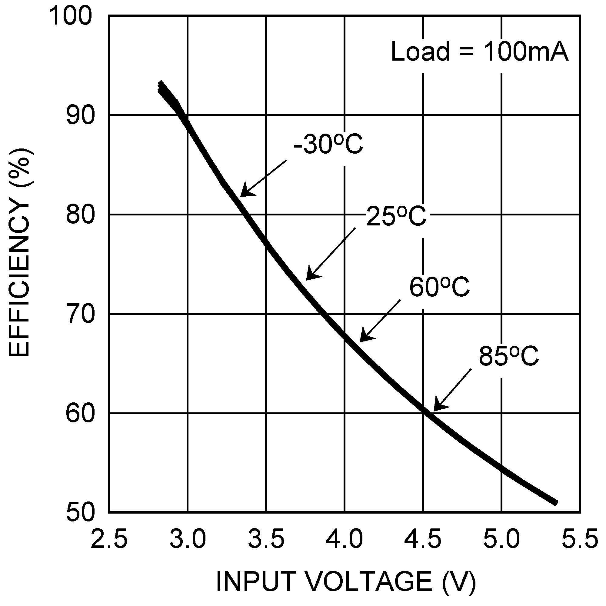
| 4.1-V Mode | ||
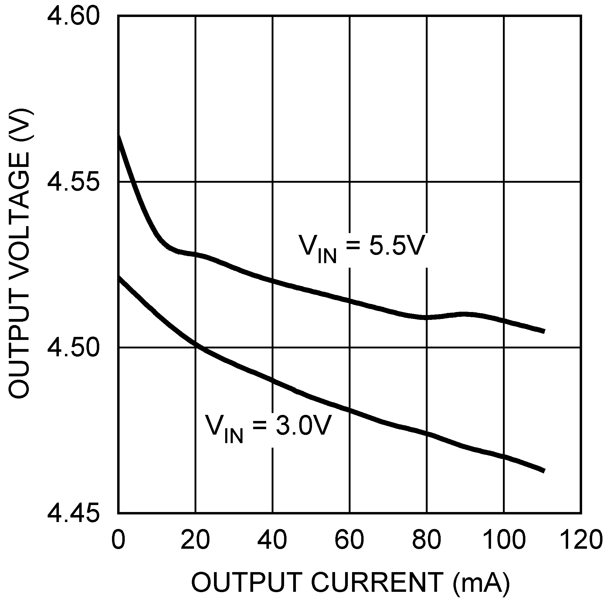
| 4.5-V Mode | ||
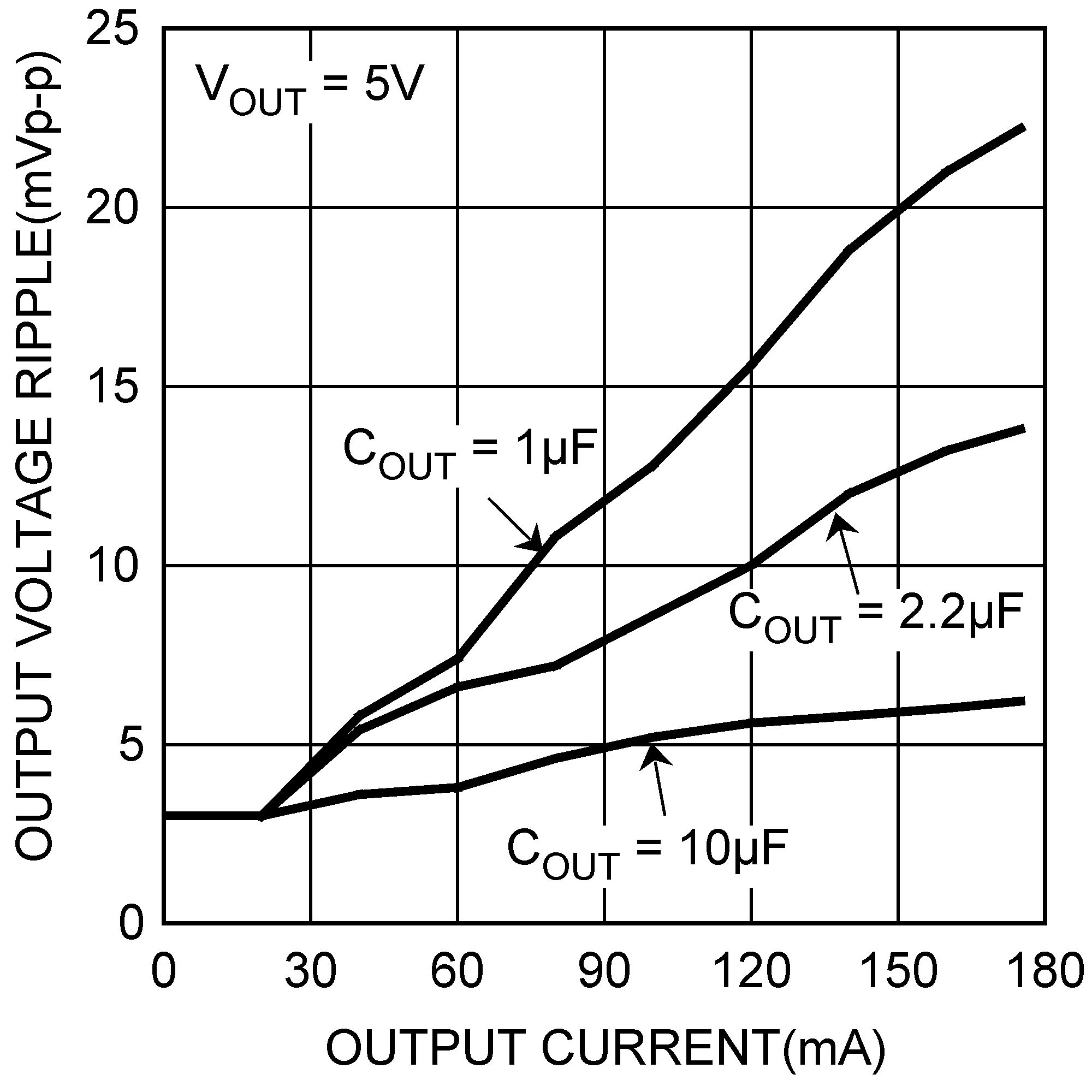
| 5-V Mode | ||
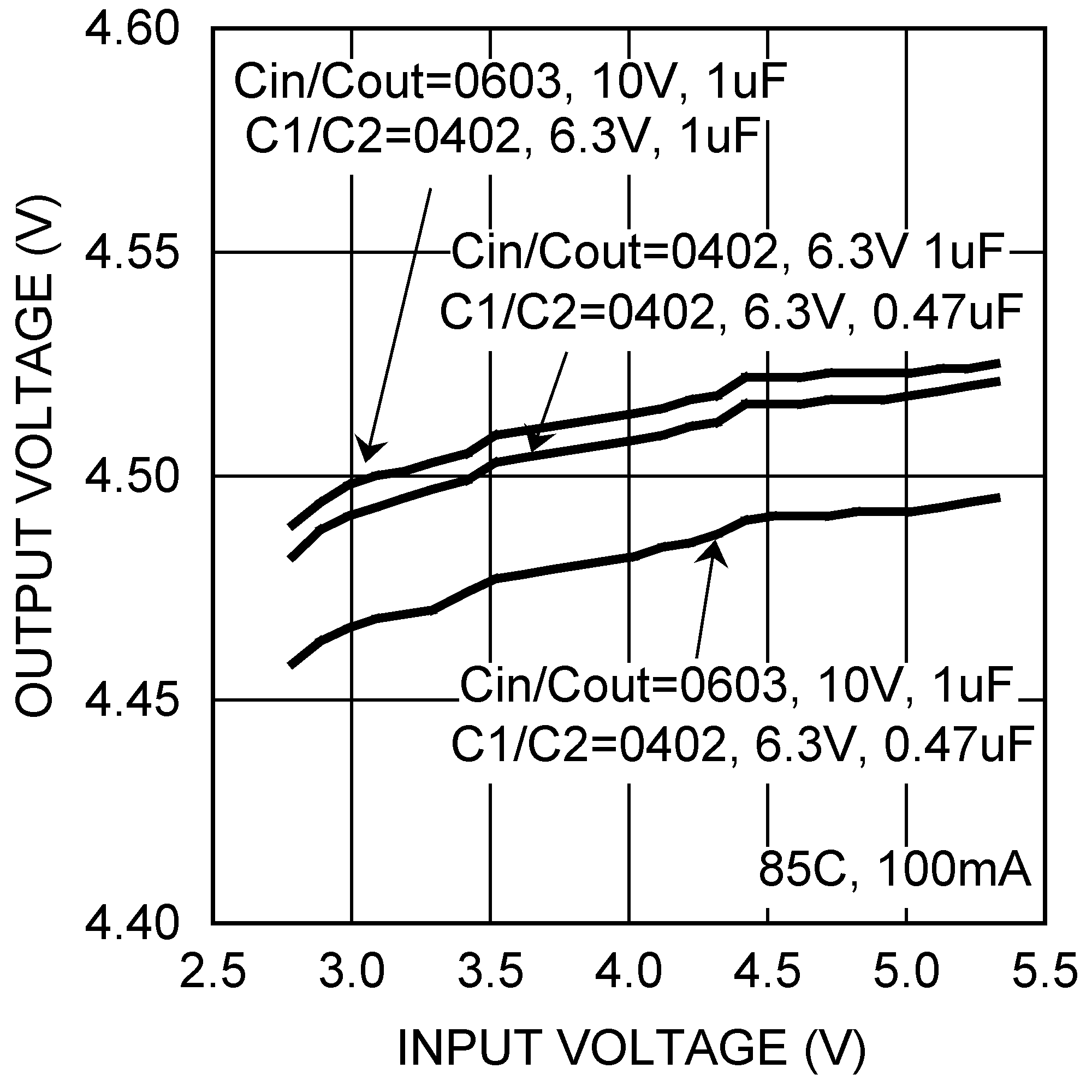
| 4.5-V Mode | ||
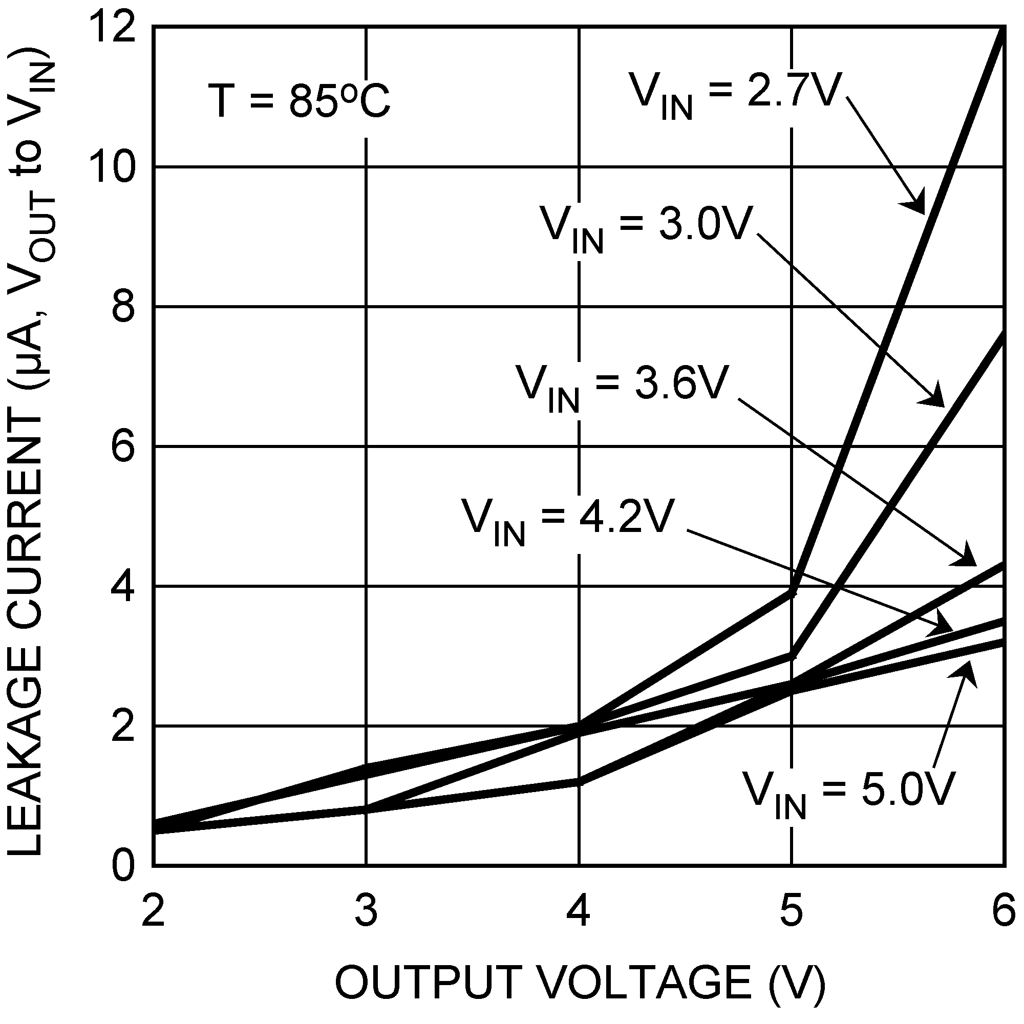
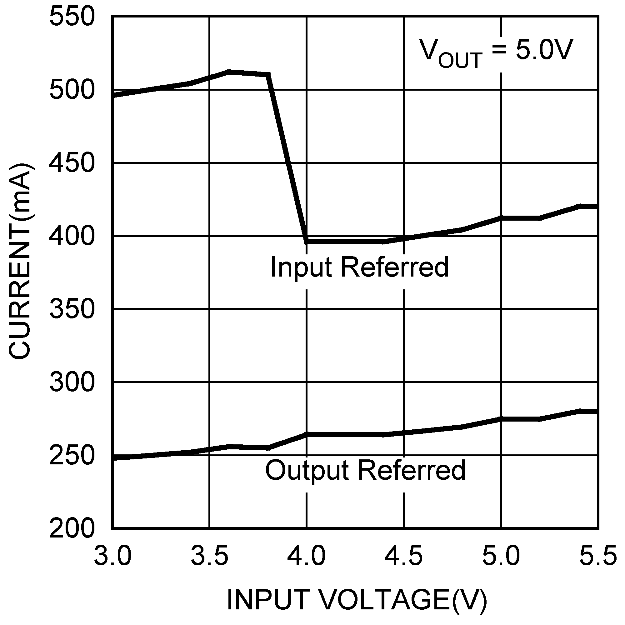
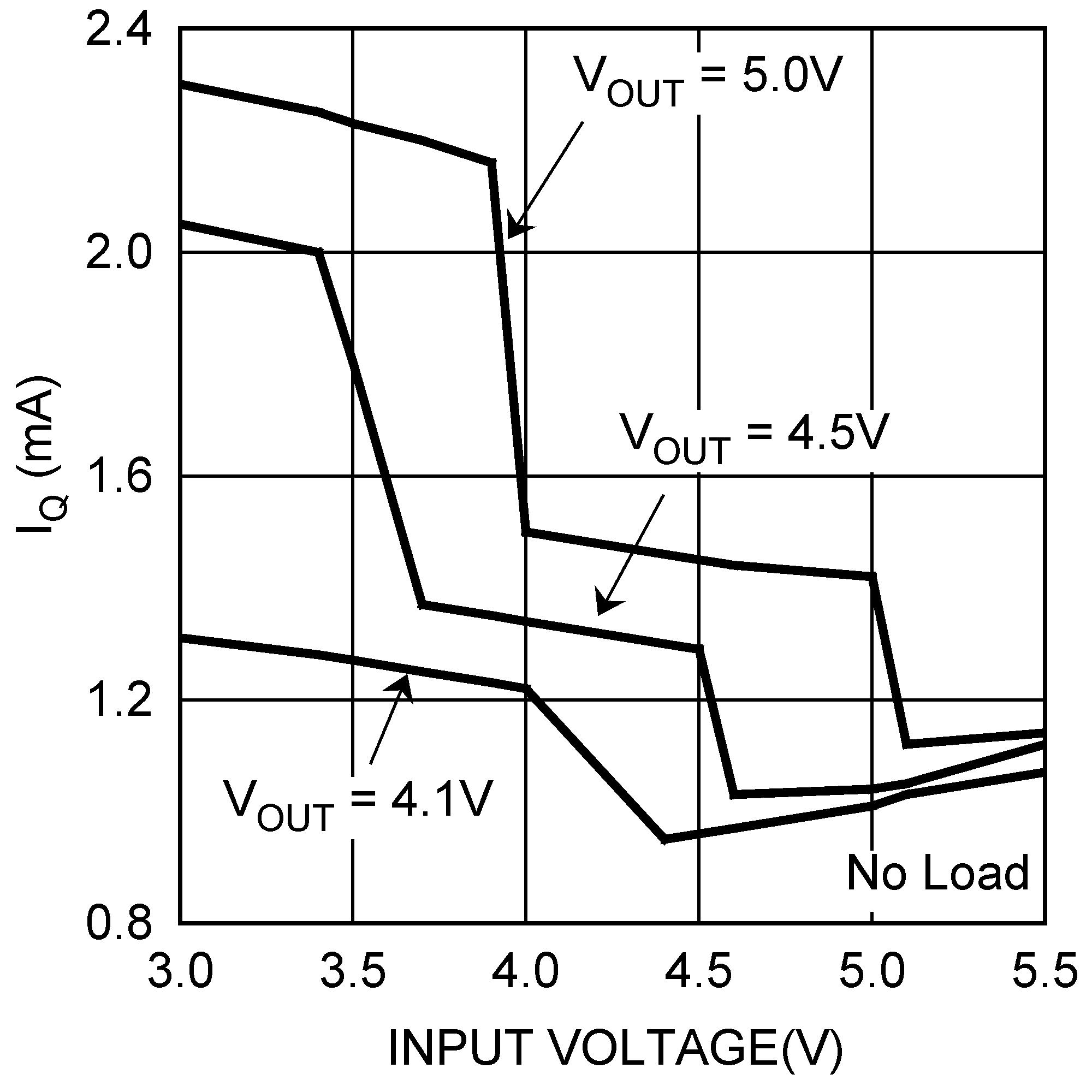
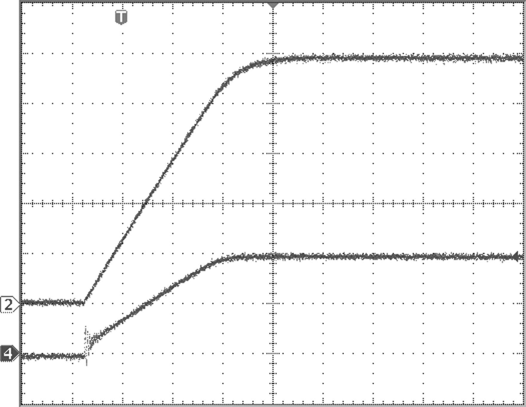
| VIN = 3.6 V | Load = 200 mA | Time scale: 100 µs/Div |
| CH2: VOUT; Scale: 1V/Div, DC Coupled | ||
| CH4: IIN; Scale: 200 mA/Div, DC Coupled | ||
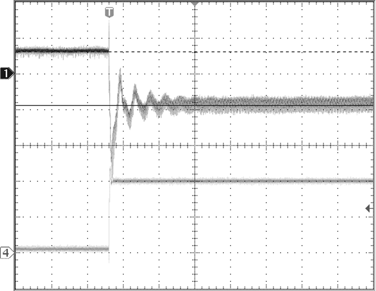
| VOUT = 5-V Mode | VBATT = 4 V | Time scale: 10 µs/Div |
| CH1: VOUT; Scale: 50mV/Div, AC Coupled | ||
| CH4: IOUT; Scale: 100mA/Div, DC Coupled | ||
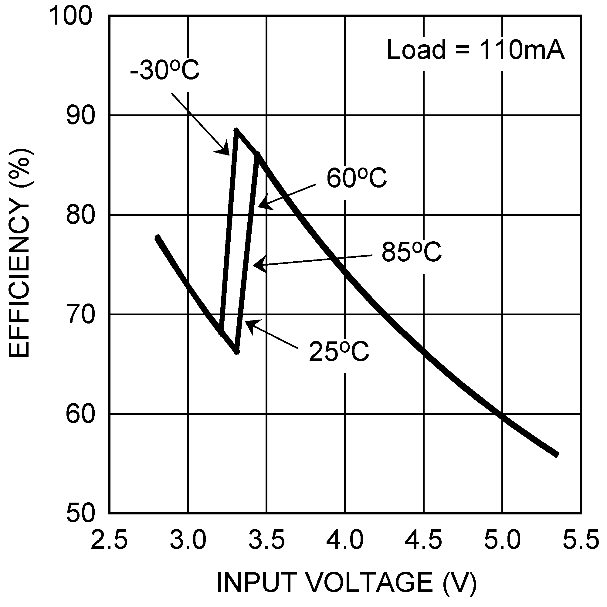
| 4.5-V Mode | ||
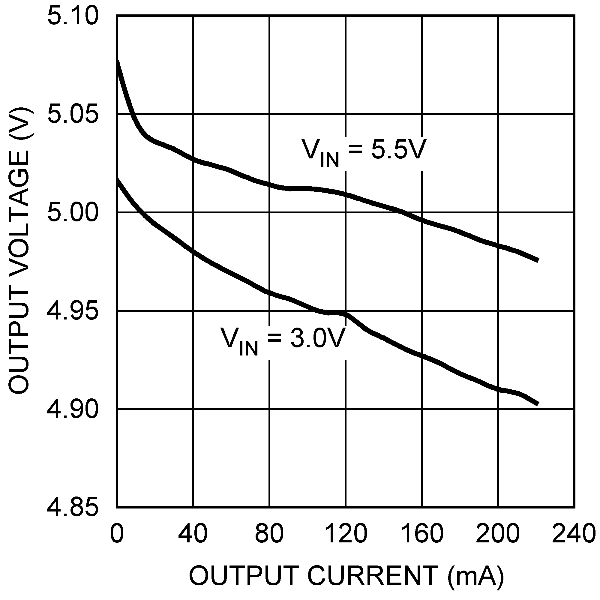
| 5-V Mode | ||
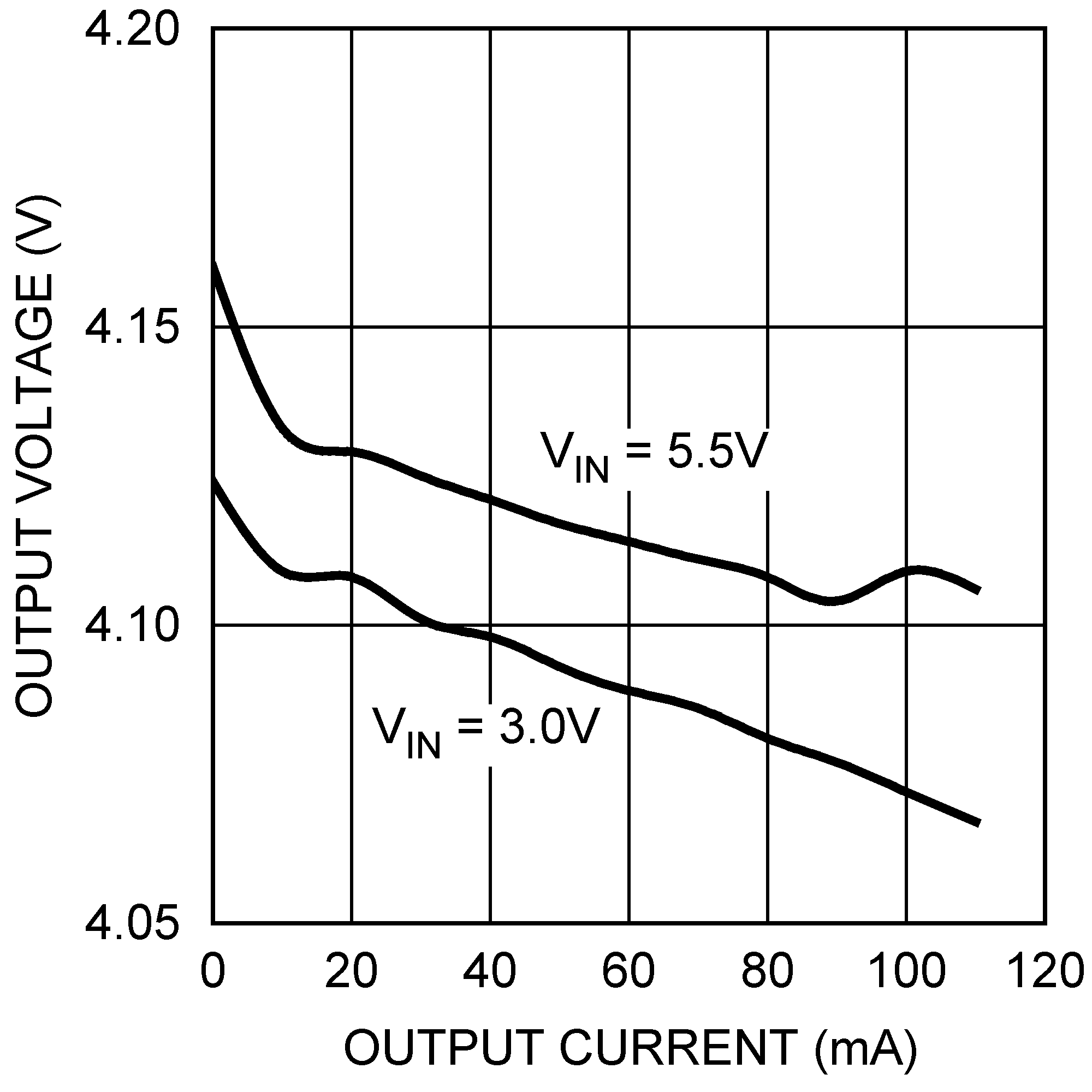
| 4.1-V Mode | ||
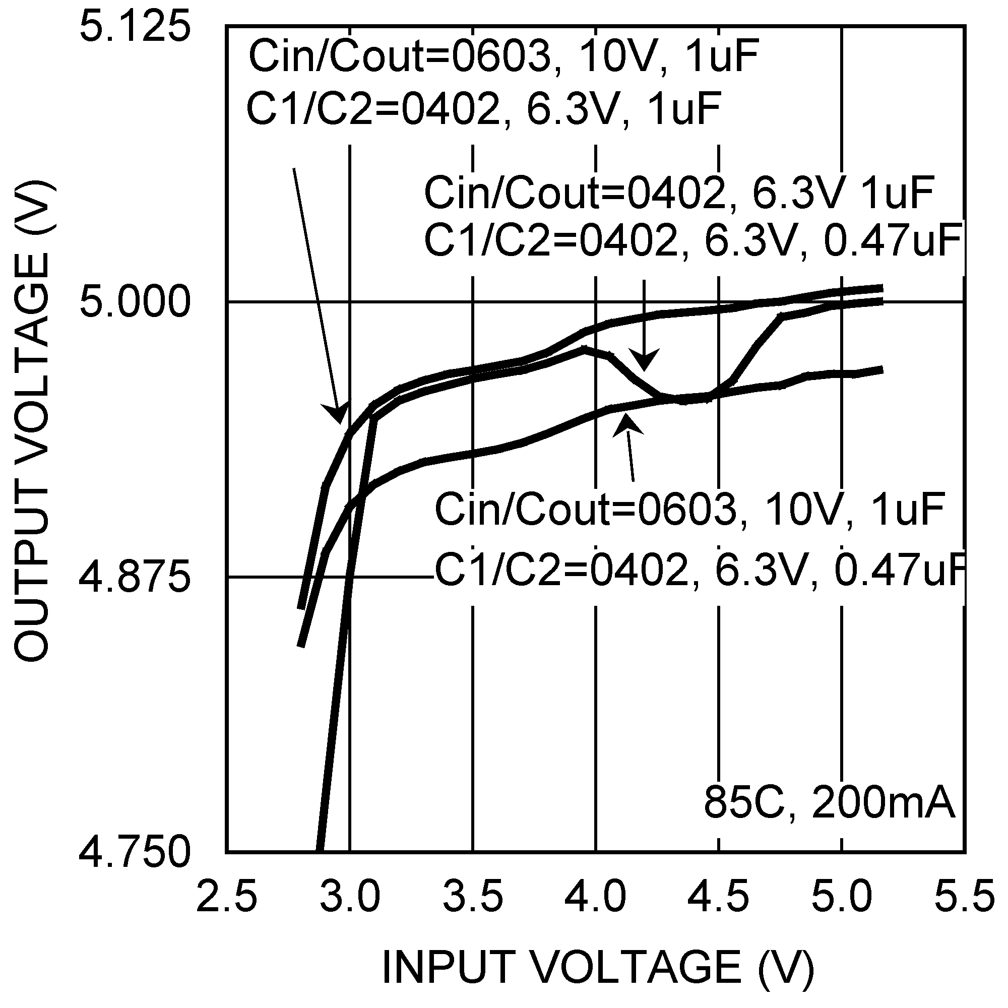
| 5-V Mode | ||
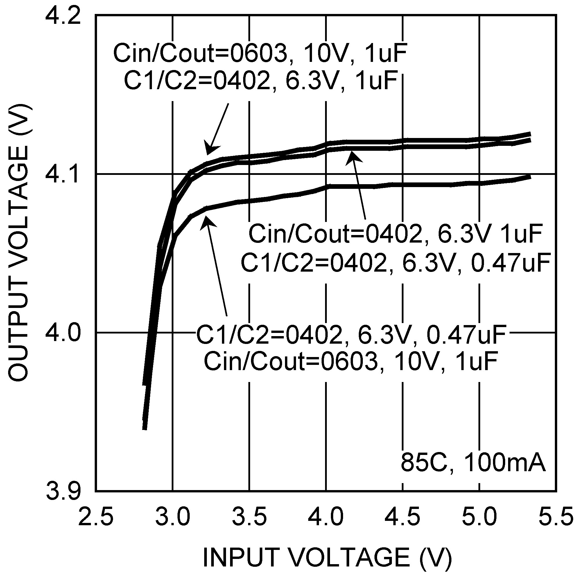
| 4.1-V Mode | ||
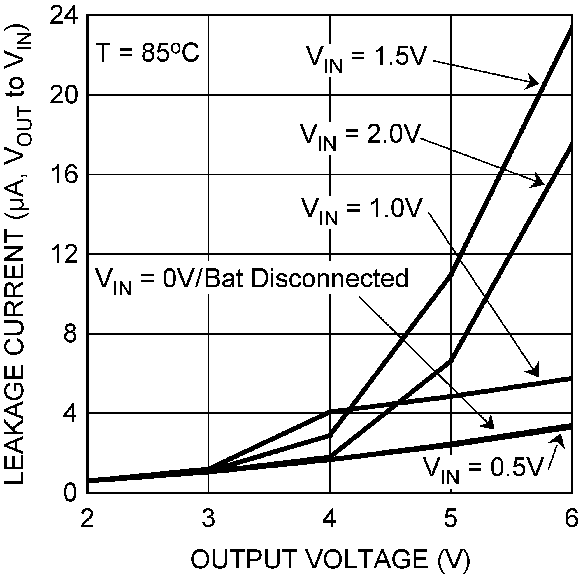
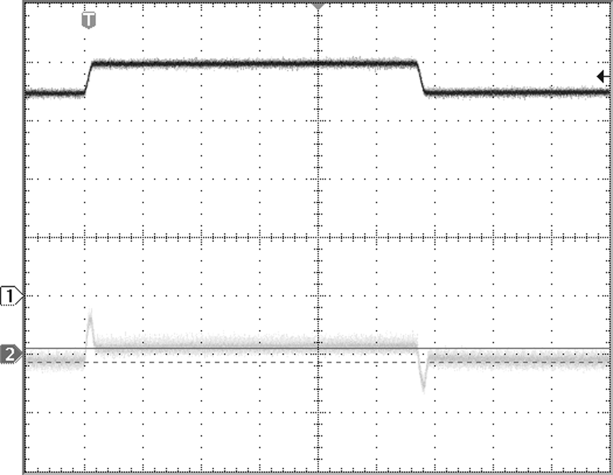
| VOUT = 5-V Mode | Load = 200 mA | Time scale: 100 µs/Div |
| CH1: VIN; Scale: 1V/Div, DC Coupled | ||
| CH2: VOUT; Scale: 100mV/Div, AC Coupled | ||
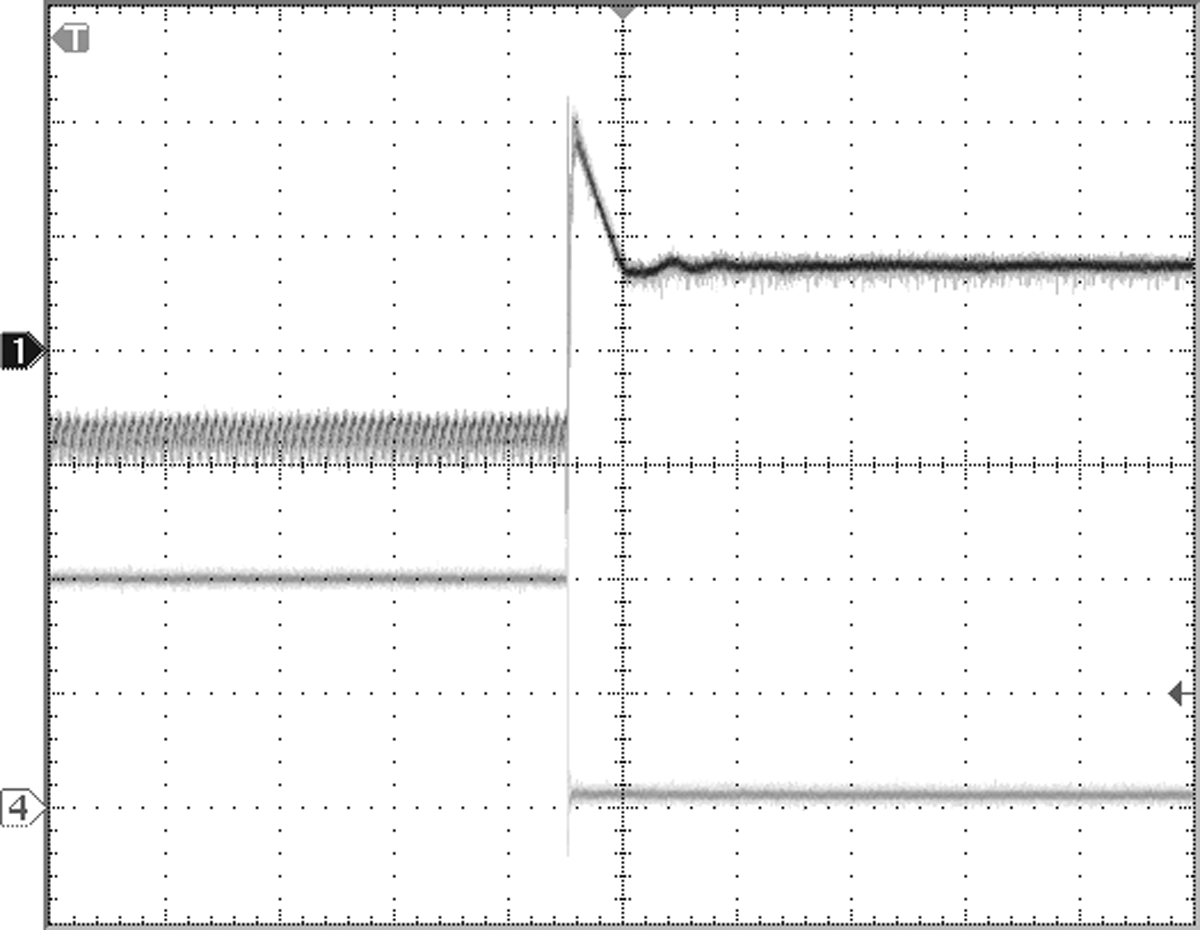
| VOUT = 5-V Mode | VBATT = 4 V | Time scale: 10 µs/Div |
| CH1: VOUT; Scale: 50mV/Div, AC Coupled | ||
| CH4: IOUT; Scale: 100mA/Div, DC Coupled | ||