SNVS550E September 2009 – January 2017 LP5523
PRODUCTION DATA.
- 1 Features
- 2 Applications
- 3 Description
- 4 Revision History
- 5 Pin Configuration and Functions
-
6 Specifications
- 6.1 Absolute Maximum Ratings
- 6.2 ESD Ratings
- 6.3 Recommended Operating Conditions
- 6.4 Thermal Information
- 6.5 Electrical Characteristics
- 6.6 Charge Pump Electrical Characteristics
- 6.7 LED Driver Electrical Characteristics
- 6.8 LED Test Electrical Characteristics
- 6.9 Logic Interface Characteristics
- 6.10 Recommended External Clock Source Conditions
- 6.11 Serial Bus Timing Parameters (SDA, SCL)
- 6.12 Typical Characteristics
-
7 Detailed Description
- 7.1 Overview
- 7.2 Functional Block Diagram
- 7.3 Feature Description
- 7.4 Device Functional Modes
- 7.5 Programming
- 7.6 Register Maps
- 8 Application and Implementation
- 9 Power Supply Recommendations
- 10Layout
- 11Device and Documentation Support
- 12Mechanical, Packaging, and Orderable Information
8 Application and Implementation
NOTE
Information in the following applications sections is not part of the TI component specification, and TI does not warrant its accuracy or completeness. TI’s customers are responsible for determining suitability of components for their purposes. Customers should validate and test their design implementation to confirm system functionality.
8.1 Application Information
The LP5523 enables up to four parallel devices together, which can drive up to 12 RGB LEDs or 36 single LEDs. Figure 26 shows the connections for two LP5523 devices for six RGB LEDs. Note that D7, D8, and D9 outputs are used for the red LEDs. The SCL and SDA lines must each have a pullup resistor placed somewhere on the line (R3 and R4; the pullup resistors are normally located on the bus master.). In typical applications, values of 1.8 kΩ to 4.7 kΩ are used, depending on the bus capacitance, I/O voltage, and the desired communication speed. INT and TRIG are open-drain pins, which must have pullup resistors. Typical values for R1 and R2 are from 120 kΩ to 180 kΩ for two devices.
8.2 Typical Applications
8.2.1 Using Two LP5523 Devices in Same Application
The LP5523 enables up to four parallel devices together, which can drive up to 12 RGB LEDs or 36 single LEDs. This diagram shows the connections for two LP5523 devices for six RGB LEDs. Note that D7, D8 and D9 outputs are used for the red LEDs. The SCL and SDA lines must each have a pullup resistor placed somewhere on the line (R3 and R4; The pullup resistors are normally located on the bus master.). In typical applications values of 1.8 kΩ to 4.7 kΩ are used, depending on the bus capacitance, I/O voltage, and the desired communication speed. INT and TRIG are open-drain pins, so they must have pullup resistors. Typical values for R1 and R2 are from 120 k to 180 k for two devices.
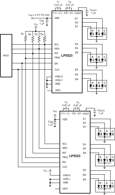 Figure 26. Typical Application Circuits
8.2.1.1 Design Requirements
| DESIGN PARAMETER | EXAMPLE VALUE |
|---|---|
| Input voltage range | 2.7 V to 5.5 V |
| LED VF (maximum) | 3.6 V |
| LED current | 25.5 mA maximum |
| Input capacitor | CIN1 = CIN2 = 1 μF |
| Output capacitor | COUT1 = COUT2 = 1 μF |
| Charge pump fly capacitors | C1 = C2 = C3 = C4 = 0.47 μF |
| Charge pump mode | 1.5× or automatic |
8.2.1.2 Detailed Design Procedure
8.2.1.2.1 Recommended External Components
The LP5523 requires 4 external capacitors for proper operation. Surface-mount multi-layer ceramic capacitors are recommended. Tantalum and aluminium capacitors are not recommended because of their high ESR. For the flying capacitors (C1 and C2) always use multi-layer ceramic capacitors. These capacitors are small, inexpensive, and have very low equivalent series resistance (ESR < 20 mΩ typical). Ceramic capacitors with X7R or X5R temperature characteristic are preferred for use with the LP5523. These capacitors have tight capacitance tolerance (as good as ±10%) and hold their value over temperature (X7R: ±15% over −55°C to +125°C; X5R: ±15% over −55°C to +85°C). Capacitors with Y5V or Z5U temperature characteristic are generally not recommended for use with the LP5523. Capacitors with these temperature characteristics typically have wide capacitance tolerance (+80%, −20%) and vary significantly over temperature (Y5V: +22%, −82% over −30°C to +85°C range; Z5U: +22%, −56% over 10°C to 85°C range). Under some conditions, a nominal 1 μF Y5V or Z5U capacitor could have a capacitance of only 0.1 μF. Such detrimental deviation is likely to cause Y5V and Z5U capacitors to fail to meet the minimum capacitance requirements of the LP5523.
For proper operation it is necessary to have at least 0.24 µF of effective capacitance for each of the flying capacitors under all operating conditions. The output capacitor COUT directly affects the magnitude of the output ripple voltage. In general, the higher the value of COUT, the lower the output ripples magnitude. For proper operation TI recommends having at least 0.50 µF of effective capacitance for CIN and COUT under all operating conditions. The voltage rating of all four capacitors must be 6.3 V; 10 V is recommended.
Table 8 lists recommended external components from some leading ceramic capacitor manufacturers. It is strongly recommended that the LP5523 circuit be thoroughly evaluated early in the design-in process with the mass-production capacitors of choice. This helps ensure that any variability in capacitance does not negatively impact circuit performance.
Table 8. Recommended External Components
| MODEL | TYPE | VENDOR | VOLTAGE RATING | PACKAGE SIZE |
|---|---|---|---|---|
| 1 µF for COUT and CIN | ||||
| C1005X5R1A105K | Ceramic X5R | TDK | 10V | 0402 |
| LMK105BJ105KV-F | Ceramic X5R | Taiyo Yuden | 10V | 0402 |
| ECJ0EB1A105M | Ceramic X5R | Panasonic | 10V | 0402 |
| ECJUVBPA105M | Ceramic X5R, array of two | Panasonic | 10V | 0504 |
| 470 nF for C1 and C2 | ||||
| C1005X5R1A474K | Ceramic X5R | TDK | 10V | 0402 |
| LMK105BJ474KV-F | Ceramic X5R | Taiyo Yuden | 10V | 0402 |
| ECJ0EB0J474K | Ceramic X5R | Panasonic | 6.3V | 0402 |
| LEDs | User defined. Note that D7, D8 and D9 outputs are powered from VDD when specifying the LEDs. | |||
8.2.1.3 Application Curves
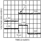
| 6 LEDs at 1 mA ,100% PWM | ||
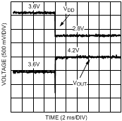
| 6 LEDs at 1 mA ,100% PWM | ||
8.2.2 Driving Haptic Feedback with LP5523
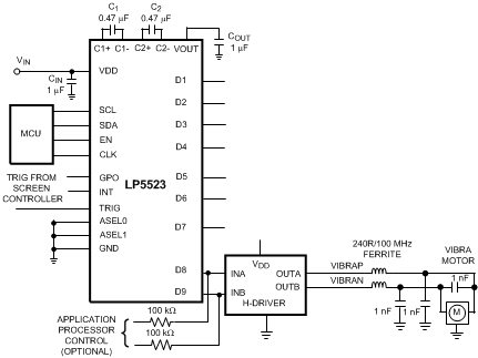 Figure 29. Example Schematic – Vibra Motor
Figure 29 depicts an example schematic for LP5523 driving a vibra motor. A vibra motor can be used for haptic feedback with touch screens and also for normal vibra operation (call indication, etc.). Battery-powered D8 and D9 outputs are used for controlling the H-driver (Microchip TC442x-series or equivalent), which drives the vibra motor. (The remaining outputs D1 to D7 can be used for LED driving, of course.) With H-driver the rotation direction of the vibra motor can be changed. For vibra operation user can load several programs to the LP5523 program memory in order to get interesting vibration effects, with changing frequency, ramps, etc.
If the application processor has controls for a vibra motor they can be connected to H-Driver INA and INB as shown in Figure 29. In this case the vibra can be controlled directly with application processor and also with LP5523. If application processor control is not needed, then the 100-kΩ resistors should be connected to GND.
A simple waveform for H-driver control is shown in Figure 30. At first the motor rotates in CW direction for 30 ms, following a rotation of 30 ms in CCW direction. The sequence is started when the TRIG signal is pulled down (active low signal). the TRIG signal is received from the touch screen controller. After the sequence is executed, the LP5523 waits for another TRIG signal to start the sequence again. TRIG signal timing is not critical; it does not have to be pulled down for the whole sequence duration like in the example. For call indication, etc. purposes the program can be changed; for example, rotation times can be adjusted to get desired haptic reaction. Direct control of D8 and D9 output is also possible through the control registers, if programming is not desired.
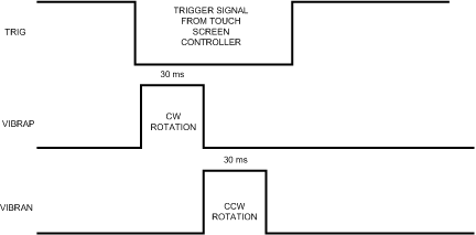 Figure 30. H-Driver Control Waveform