SNVS902A October 2012 – October 2015 TPS92640 , TPS92641
PRODUCTION DATA.
- 1 Features
- 2 Applications
- 3 Description
- 4 Revision History
- 5 Pin Configuration and Functions
- 6 Specifications
-
7 Detailed Description
- 7.1 Overview
- 7.2 Functional Block Diagram
- 7.3
Feature Description
- 7.3.1 Controlled On-Time Architecture
- 7.3.2 Switching Frequency
- 7.3.3 Average LED Current
- 7.3.4 Analog Dimming and True-Zero Operation
- 7.3.5 Undervoltage Lockout (UVLO)
- 7.3.6 PWM Dimming Using the UDIM Pin
- 7.3.7 External Shunt FET PWM Dimming
- 7.3.8 VCC Regulation and Start-up
- 7.3.9 Precision Reference
- 7.3.10 Control Loop Compensation
- 7.3.11 Overcurrent Protection
- 7.3.12 Overvoltage Protection (OVP)
- 7.3.13 Boot Undervoltage Lockout (UVLO)
- 7.4 Device Functional Modes
-
8 Application and Implementation
- 8.1 Application Information
- 8.2
Typical Applications
- 8.2.1
TPS92640: Design Procedure
- 8.2.1.1 Design Requirements
- 8.2.1.2
Detailed Design Procedure
- 8.2.1.2.1 Set Output Voltage Feedback Ratio
- 8.2.1.2.2 Set Switching Frequency
- 8.2.1.2.3 Set Average LED Current
- 8.2.1.2.4 Set Inductor Ripple Current
- 8.2.1.2.5 Set LED Ripple Current and Determine Output Capacitance, COUT
- 8.2.1.2.6 Choose N-Channel MOSFETs
- 8.2.1.2.7 Choose Input Capacitance
- 8.2.1.2.8 Set the Turnon Voltage and Undervoltage Lockout Hysteresis
- 8.2.2
TPS92640 - PWM Dimming Application
- 8.2.2.1 Design Requirements
- 8.2.2.2
Detailed Design Procedure
- 8.2.2.2.1 Calculate Operating Points
- 8.2.2.2.2 Output Voltage Feedback
- 8.2.2.2.3 Switching Frequency
- 8.2.2.2.4 Set the Feedback Reference and LED Current
- 8.2.2.2.5 Calculate the Inductor Value
- 8.2.2.2.6 Calculate the Output Capacitor Value
- 8.2.2.2.7 Calculate the MOSFET Parameters
- 8.2.2.2.8 Calculate the Minimum Input Capacitance
- 8.2.2.2.9 Undervoltage Lockout and Hysteresis
- 8.2.2.3 Application Curve
- 8.2.1
TPS92640: Design Procedure
- 9 Power Supply Recommendations
- 10Layout
- 11Device and Documentation Support
- 12Mechanical, Packaging, and Orderable Information
7 Detailed Description
7.1 Overview
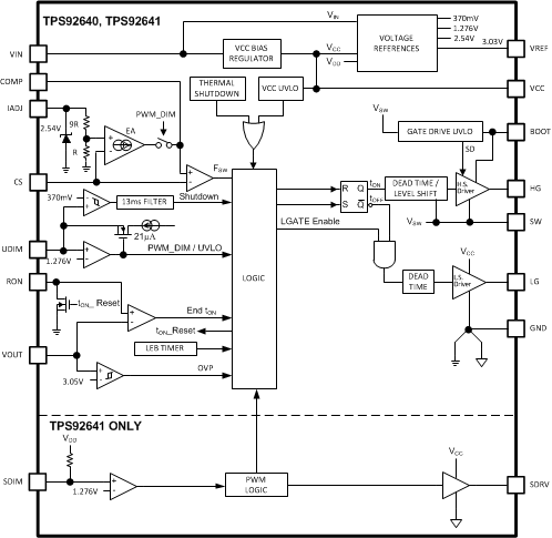
The TPS92640 and TPS92641 devices are synchronous N-channel MOSFET (NFET) controllers for step-down (buck) current regulators, which are ideal for driving LED loads. They can accept wide input voltage range allowing for greater flexibility in powering different series connected LED string combinations. The single current sense pin with low adjustable threshold voltage provides an excellent method for regulating LED current while maintaining high system efficiency. The TPS92640 and TPS92641 devices use valley current control with a controlled on-time architecture that allows the converter to be operated at nearly constant switching frequency without the need for slope compensation. The extremely accurate adjustable current sense threshold together with the synchronous operation provides the capability to amplitude (analog) dim the LED current with high contrast ratios. Excellent PWM dimming is attainable using the main NFETs or the external shunt FET driver (TPS92641 only). The TPS92640 and TPS92641 devices incorporate 2-Ω, 1-A internal gate drivers and supports constant current operation up to 5 A. This simple controller contains all the features necessary to implement a high-efficiency, versatile LED driver with precise dimming response.
7.2 Functional Block Diagram
7.3 Feature Description
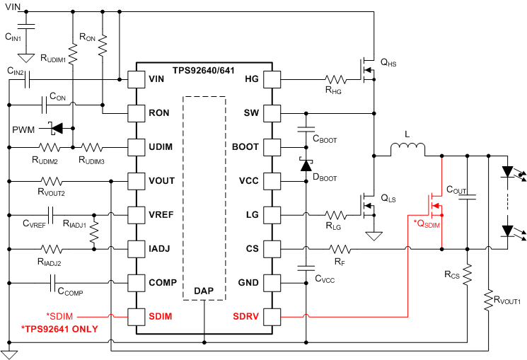 Figure 13. Synchronous Buck LED Driver
7.3.1 Controlled On-Time Architecture
The control architecture is a combination of valley current control and a one-shot on-timer that varies with input and output voltage. The TPS92640 and TPS92641 devices use a series resistor in the LED path to sense both average LED current and valley inductor current. During the time that the high side NFET is turned on (tON), the input voltage charges up the inductor. When it is turned off (tOFF) and the low side NFET is turned on, the inductor discharges. During both intervals, the current is supplied to the load keeping the LEDs forward biased. Figure 14 shows the inductor current (iL) waveform for a buck converter operating in continuous conduction mode (CCM). As the system changes input voltage or output voltage, duty cycle D is varied indirectly by changing both tON and tOFF to regulate IL and ultimately ILED. For any buck regulator, duty cycle, D, is calculated using Equation 1.

where
- VCS is the voltage measured at the CS pin of the IC and η is the estimated or actual converter efficiency.
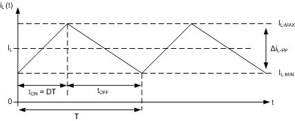 Figure 14. Ideal CCM Buck Converter Inductor Current IL Waveform
7.3.2 Switching Frequency
The on-time is determined based on the external resistor (RON) connected between RON and VIN pins in combination with a capacitor (CON) between RON and GND pins. The input voltage and the RON resistor set the current sourced into the RON capacitor which governs the ramp speed. The ramp threshold is proportional to scaled down feedback of VOUT at VOUT pin. The proportionality of VOUT is set by an external resistor divider (RVOUT1, RVOUT2) from VOUT. The switching frequency, fSW can be calculated based on on-time and off-time using Equation 2.
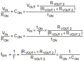
Even though the on-time control is quasi-hysteretic, the input and output voltage proportionality creates a nearly constant switching frequency over the entire operating range. Quasi-hysteretic control minimizes the control loop compensation necessary in many switching regulators, simplifying the design process. It also mitigates current mode instability (also known as sub-harmonic oscillation) found in standard fixed frequency current mode control when operating near or above 50% duty cycle. The inductor current sensing and averaging mechanism in the valley detection control loop provides highly accurate LED current regulation over the entire operating range and temperature.
7.3.3 Average LED Current
Average LED current regulation is set using a sense resistor in series with the LEDs. The internal error-amplifer regulates the voltage across the sense resistor (VCS) to the IADJ voltage divided by 10. The error amplifier input offset voltage has been minimized using auto-zero calibration technique as shown in . In this chopping scheme, the noninverting and inverting inputs and outputs change polarity every switching cycle to cancel the offset, providing near zero input offset voltage.
 Figure 15. Working Principle of the Chopper OTA to Minimize Input Offset Voltage
IADJ can be set to any value up to 2.54 V by connecting it to VREF through a resistor divider for static output current settings. IADJ can also be used to change the regulation point if connected to a controlled voltage source or potentiometer to provide analog dimming. It is also possible to configure IADJ to be used for thermal foldback functions.


7.3.4 Analog Dimming and True-Zero Operation
In traditional Buck converters, discontinuous conduction mode (DCM) operation of inductor current results in loss of linearity at low dimming levels and limits the analog dimming range. When using TPS92640 and TPS92641 devices to implement synchronous buck converter, the inductor current is forced to maintain continuous conduction mode (CCM). As a result, it is possible to maintain linearity and achieve true-zero LED current operation with respect to analog dimming command. For true zero application, an external capacitor is required across the LED string to provide a negative current path for the inductor current loop. Figure 16 shows the inductor current (IL) and output voltage (VOUT) waveform for a buck converter operating at true zero average current level.
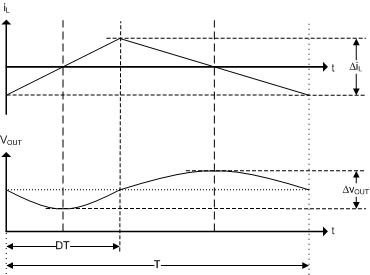 Figure 16. True Zero CCM Buck Converter Inductor Current IL and Output Voltage VOUT Waveform
In true zero application (VIADJ=0 V), there will be a certain amount of ILED passing the LEDs even though the average inductor current is well-regulated at 0-A set-point. The shaped area in Figure 17 shows the current that will pass through the LED string (iLED).
 Figure 17. Output Current Waveform in True Zero Application with VIADJ = 0 V
An external resistor, ROFF as shown in Figure 18 is recommended from VOUT to CS to shunt the positive current ripple while maintaining the operation of error amplifier to cancel input offset voltage. The shunt current (IOFF) should be at least half of the output current ripple to ensure proper operation.
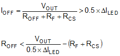
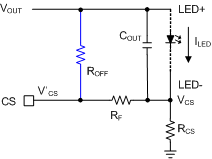 Figure 18. ROFF for True Zero Application
The resistor ROFF also impacts the start-up behavior of the circuit as it creates an DC shift in the voltage sensed at CS pin. To ensure proper start-up sequence and monotonic LED current behavior, the voltage V'CS should exceed a threshold voltage based on the native offset of the error amplifier before VOUT exceeding the LED forward voltage, VLED. Assuming a worst case native off-set (non-chopping) of error amplifier to be less than ±10 mV, the voltage V'CS must be greater than this threshold to initiate switching and auto-zero operation. Therefore, ROFF should be sized to also meet following condition.
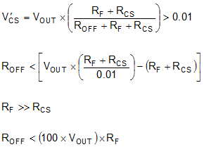
To conclude, an external resistor (ROFF) from VOUT to CS pin is required for true zero application, where ROFF should be:

7.3.5 Undervoltage Lockout (UVLO)
The UDIM pin of the TPS92640 and TPS92641 devices is a dual function input that features an accurate 1.276-V threshold with programmable hysteresis. This pin functions as both the PWM dimming input of the LEDs and as an input UVLO with built-in hysteresis. When the pin voltage rises and exceeds the 1.276-V threshold, 21 µA (typical) of current is driven out of the UDIM pin into the resistor divider (RUDIM1, RUDIM2) providing programmable hysteresis. The UVLO turnon threshold, VTURN-ON, is defined using Equation 8.

Once the input voltage is above VTURN_ON, the current source is active and the UVLO hysteresis is determined by Equation 9.

When using the UDIM pin for UVLO and PWM dimming concurrently, the UVLO circuit can have an extra resistor (RUDIM3) to set the hysteresis. This allows the standard resistor divider to have smaller values minimizing delays that can incur with additional external PWM dimming circuitry. In general, at least 3 V of hysteresis is preferable when PWM dimming if operating near the UVLO threshold. Under these conditions, the UVLO hysteresis is defined using Equation 10.

7.3.6 PWM Dimming Using the UDIM Pin
The UDIM pin can be driven with a PWM signal, which controls the synchronous NFET operation. The brightness of the LEDs can be varied by modulating the duty cycle (DDIM) of this signal using a Schottky diode with anode connected to UDIM pin, as shown in Figure 13.
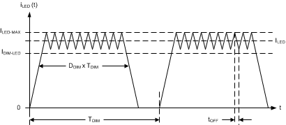 Figure 19. LED Current During UDIM Pin PWM Dimming
Figure 19 shows the LED current waveform during PWM dimming where duty cycle (DDIM) is the percentage of the dimming period (TDIM) that the synchronous NFETs are switching. For the remainder of TDIM, the NFETs are disabled. The resulting dimmed LED current (IDIM_LED) is:

7.3.7 External Shunt FET PWM Dimming
Extremely high dimming range and linearity can be achieved by using TPS92641 device for Shunt FET dimming operation with SDIM and SDRV pin. When higher frequency and time resolution PWM dimming signal is applied to the SDIM pin, the SDRV pin provides an inverted signal of the same frequency and duty cycle that can be used to drive the gate of a Shunt NFET directly across the LED load. Because the output voltage will go to near zero when the Shunt NFET is turned on, the internal on-timer at the RON pin will switch to a fixed minimum on-time during the off-time of the dimming cycle. This method keeps the inductor current slewed up and the converter regulating, without the presence of extremely high switching frequencies. During the on-time of the dimming cycle, the converter will switch in its regular fashion with the programmed on-time at the RON pin. An internal resistor pulls the SDIM pin to logic high if left open. In this case, the SDRV driver will be off.
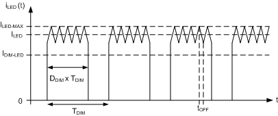 Figure 20. Ideal LED Current During Shunt FET PWM Dimming
Figure 20 shows the ideal LED current waveform during Shunt FET PWM dimming which is very similar to the internal PWM dimming described and shown previously except with much faster rise and fall of the LED current. With this method, only the speed of the parallel Shunt NFET limits the dimming frequency and dimming duty cycle.
7.3.8 VCC Regulation and Start-up
The TPS92640 and TPS92641 devices include a high voltage, low-dropout bias regulator. When power is applied, the regulator is enabled and sources current into an external capacitor (CVCC) connected to the VCC pin. The recommended bypass capacitance for the VCC regulator is 2.2 µF to 3.3 µF. This capacitor should be rated for 10 V or greater and an X7R dielectric ceramic is recommended. The output of the VCC regulator is monitored by an internal UVLO circuit that protects the device from attempting to operate with insufficient supply voltage, and the supply current is also internally current-limited. When VIN is close or lower than 8.5 V, the regulator will enter the by-pass mode and the VCC will closely follow VIN. This linear regulator is the primary heat source generator of the device. The amount of heat generated is a function of input voltage (VIN), switching frequency (FSW) and the characteristics of the power MOSFET used. The thermal handling capability of the device imposes a limit on the maximum switching frequency can be used, especially when VIN is higher than 48 V and high current power MOSFET is used.
7.3.9 Precision Reference
The device includes a precision 3-V reference. This can be used in conjunction with a resistor divider to set voltage levels for the IADJ pin and other external circuitry requiring a reference. It can also be used to supply current to low power micro-controllers. The source current capability from VREF pin is internally limited 2.1 mA. For the VREF regulator, TI recommends a bypass capacitance from 0.1 µF to 1 µF.
7.3.10 Control Loop Compensation
Compensating the TPS92640 and TPS92641 devices is relatively simple for most applications. The only compensation needed is a compensation capacitor, CCOMP across the COMP pin and ground to place a low-frequency dominant pole in the system. The pole must be placed low enough to ensure adequate phase margin at the crossover frequency. For most of the applications, CCOMP of 100 nF to 470 nF is good enough. Additionally, TI recommends a high quality ceramic capacitor with X7R dielectric rated for 25 V.
7.3.11 Overcurrent Protection
The TPS92640 and TPS92641 devices has overcurrent protection to protect the high side NFET (HS-NFET) along with the rest of the system from overcurrent conditions. This peak current limit of 1.28 V (with VIN = 85 V at room temperature) is sensed across the high side FET RDS-ON (from SW to VIN). If the threshold is reached or exceeded, HS-NFET will turn off and the low side NFET (LS-NFET) will turn on for approximately 800 ns. Then HS-NFET will turn on again, if the threshold is still reached or exceeded, both FETs are shutoff for 270-µs typical. Figure 21 shows the waveforms of HG and LG under overcurrent protection.
 Figure 21. HG and LG Waveforms Under Overcurrent Protection
7.3.12 Overvoltage Protection (OVP)
The TPS92640 and TPS92641 devices have programmable overvoltage protection by using the resistor divider at the VOUT pin. The OVP limit, VOVP_ON, is defined using Equation 12.

If the output voltage reaches VOVP_ON, the HG, LG and SDRV pins are pulled low to prevent damage to the LEDs or the rest of the circuit. The OVP circuit has a fixed hysteresis of 100 mV before the driver attempts to switch again.
7.3.13 Boot Undervoltage Lockout (UVLO)
The BOOT UVLO circuit is implemented to ensure proper operation of the high-side gate driver under all operating conditions. The switching operation is commenced once the BOOT voltage exceeds 3.4 V above the SW pin. Comparator hysteresis of 1.8 V is included to prevent false tripping due to high-frequency switching noise. When the BOOT falls below the low voltage threshold (1.6 V typical), the high side NFET is disabled by pulling HG pin to SW pin. The next turnon transition of low-side NFET pulls SW pin down and charges the BOOT capacitor (CBOOT) through VCC. Normal operation is commenced once BOOT capacitor (CBOOT) is charged above BOOT UVLO turnon threshold of 3.4 V.
The boostrap circuit behavior impacts the circuit behavior near dropout (VIN= VOUT) conditions. A minimum off-time is implemented to restrict the maximum duty cycle and maintain charge on the external BOOT capacitor, CBOOT. As the input voltage, VIN, approachs close to the output voltage, VOUT, the output current will fall with the switching frequency, as in conventional Buck regulator. This behavior ensures smooth operation in and out of dropout region while ensuring proper operation of high side gate driver and bootstrap circuit.
7.4 Device Functional Modes
7.4.1 Low Power Shutdown Using the UDIM Pin
The TPS92640 and TPS92641 devices can be placed into a low power shutdown mode by grounding the UDIM pin directly (any voltage below 370 mV) for more than 13 ms (typical).
7.4.2 Thermal Shutdown
Internal thermal shutdown circuitry is provided to protect the device in the event that the maximum junction temperature is exceeded. The threshold for thermal shutdown is 165°C with a 20°C hysteresis (both values typical). During thermal shutdown the NFETs and drivers are disabled.