SNVSA72 February   2015 LP8728D-Q1

PRODUCTION DATA.  

  1. Features
  2. Applications
  3. Description
  4. Revision History
  5. Pin Configuration and Functions
  6. Specifications
    1. 6.1 Absolute Maximum Ratings
    2. 6.2 ESD Ratings
    3. 6.3 Recommended Operating Conditions
    4. 6.4 Thermal Information
    5. 6.5 Electrical Characteristics
    6. 6.6 System Characteristics
    7. 6.7 Typical Characteristics
  7. Detailed Description
    1. 7.1 Overview
    2. 7.2 Functional Block Diagram
    3. 7.3 Feature Description
      1. 7.3.1 Buck Information
        1. 7.3.1.1 Features
      2. 7.3.2 Thermal Shutdown (TSD)
      3. 7.3.3 Undervoltage Lockout (UVLO)
      4. 7.3.4 Overvoltage Protection (OVP)
    4. 7.4 Device Functional Modes
      1. 7.4.1 Shutdown Mode
      2. 7.4.2 Active Mode
  8. Application and Implementation
    1. 8.1 Application Information
    2. 8.2 Typical Application
      1. 8.2.1 Design Requirements
      2. 8.2.2 Detailed Design Procedure
        1. 8.2.2.1 Inductor
        2. 8.2.2.2 Input and Output Capacitors
      3. 8.2.3 Application Performance Plots
  9. Power Supply Recommendations
  10. 10Layout
    1. 10.1 Layout Guidelines
    2. 10.2 Layout Example
  11. 11Device and Documentation Support
    1. 11.1 Device Support
      1. 11.1.1 Third-Party Products Disclaimer
    2. 11.2 Related Documentation
    3. 11.3 Trademarks
    4. 11.4 Electrostatic Discharge Caution
    5. 11.5 Glossary
  12. 12Mechanical, Packaging, and Orderable Information

10 Layout

10.1 Layout Guidelines

  • AVDD and BYP pins must be bypassed to ground. 1-µF ceramic capacitor is recommended. Place the capacitors close to the AVDD, BYP, and AGND pins.
  • AGND pin must be tied to the PCB ground plane. Use multiple vias to minimize the inductance.
  • AVDD pin must be connected to PCB VIN plane. Use multiple vias to minimize the inductance.
  • Place the buck converter input capacitors as close to the buck input voltage and buck ground pins as possible.
  • Place the buck converter output capacitors and inductors so that the buck converter switching loops can be routed on top layer. Try to minimize the area of the switching loops.
  • Keep the trace width from switch pin to inductor wide enough to withstand the switching currents. Avoid any excess copper on the switch node to minimize parasitic switch node capacitance.
  • Connect the exposed thermal pad to ground plane with multiple thermal vias.
  • Avoid routing digital signals directly under the switching loops to avoid interferences.

10.2 Layout Example
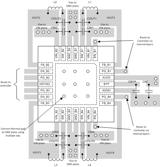
LP8728_Layout_Example.gifFigure 21. LP8728D-Q1 Layout Example