-
TPS61177A WLED Driver for Notebooks With PWM Interface and Mixed Dimming Mode
- 1 Features
- 2 Applications
- 3 Description
- 4 Revision History
- 5 Pin Configuration and Functions
- 6 Specifications
-
7 Detailed Description
- 7.1 Overview
- 7.2 Functional Block Diagram
- 7.3
Feature Description
- 7.3.1 Supply Voltage
- 7.3.2 Boost Regulator
- 7.3.3 Programmable Switch Frequency and Slew Rate
- 7.3.4 LED Current Sinks
- 7.3.5 Enable and Start-Up Timing
- 7.3.6 Input Undervoltage Protection (UVLO)
- 7.3.7 Overvoltage Protection (OVP)
- 7.3.8 Current-Sink Open Protection
- 7.3.9 Overcurrent Protection
- 7.3.10 Thermal Protection
- 7.4 Device Functional Modes
- 7.5 Programming
- 7.6
Register Maps
- 7.6.1 MODE (A0h)
- 7.6.2 CS (A1h)
- 7.6.3 UVLO (A2h)
- 7.6.4 FREQ (A3h)
- 7.6.5 SR (A4h)
- 7.6.6 ILIM (A5h)
- 7.6.7 Control (FFh)
- 7.6.8 Example - Writing to a Single RAM Register
- 7.6.9 Example - Writing to Multiple RAM Registers
- 7.6.10 Example - Saving Contents of all RAM Registers to E2PROM
- 7.6.11 Example - Reading from a Single RAM Register
- 7.6.12 Example - Reading from a Single E2PROM Register
- 7.6.13 Example - Reading from Multiple RAM Registers
- 7.6.14 Example - Reading from Multiple E2PROM Registers
- 8 Application and Implementation
- 9 Power Supply Recommendations
- 10Layout
- 11Device and Documentation Support
- 12Mechanical, Packaging, and Orderable Information
- IMPORTANT NOTICE
TPS61177A WLED Driver for Notebooks With PWM Interface and Mixed Dimming Mode
1 Features
- 2.5-V to 24-V Input Voltage Range
- 39-V Maximum Output Voltage
- Integrated 1.8-A, 40-V MOSFET
- 450-kHz to 1.2-MHz Programmable Switching Frequency
- Adaptive Boost Output to WLED Voltages
- 100-Hz to 25-kHz Wide Input PWM Dimming Frequency Range
- 1% Minimum Dimming Duty Cycle
- Small External Components
- Integrated Loop Compensation
- Six Current Sinks of 30 mA Maximum
- 1% (Typical) Current Matching
- Input PWM Glitch Filter
- PWM Brightness Interface Control
- Three Optional Dimming Methods, including Direct PWM Dimming, Analog Dimming, and Analog and PWM Mixed Dimming
- Built-in WLED Open Protection
- Thermal Shutdown
2 Applications
- Notebook and Tablet LCD Display Backlights
- Patient Monitors
- Medical Displays
- HMI
- Test and Measurement Equipment
3 Description
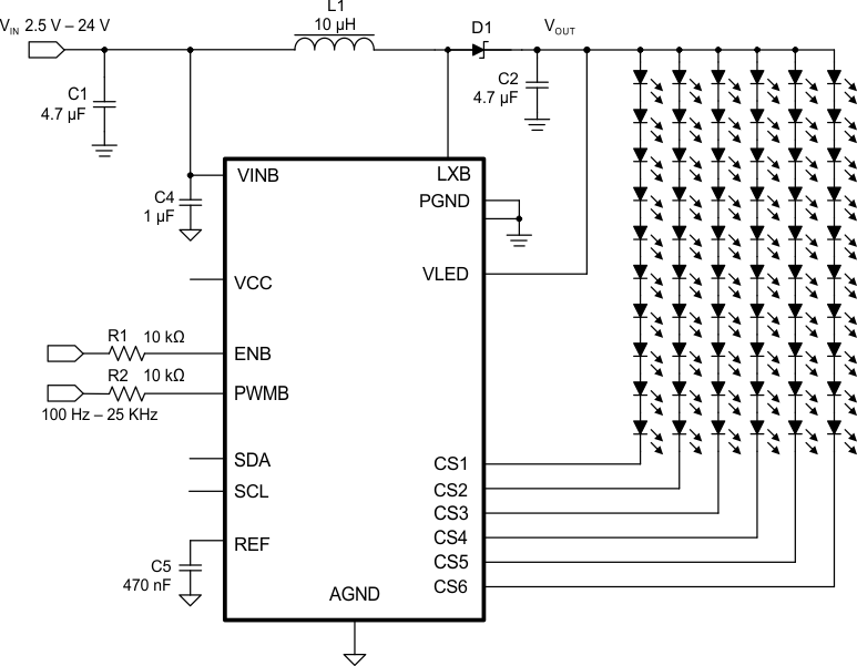
The TPS61177A device provides a highly integrated white LED (WLED) driver solution for notebook LCD backlight. This device has a built-in high-efficiency boost regulator with integrated 1.8-A, 40-V power MOSFET. The six current sink regulators provide high precision current regulation and matching. In total, the device can support up to 72 WLEDs. In addition, the boost output automatically adjusts its voltage to the WLED forward voltage to optimize efficiency.
The TPS61177A supports the analog dimming, analog and PWM dimming, and direct PWM dimming method. During analog dimming mode, each CS current linearly varies depending on the duty cycle information on the PWMB pin. During analog and PWM mixed dimming mode, the input PWM duty cycle information is translated to an analog signal to control the WLED current linearly over 25% to 100% brightness area. The device also allows adding PWM dimming when the analog current is down to 25%. Below 25%, the analog signal translates to PWM duty cycle information to control the on or off of WLED current and averages the WLED current down to 1%. The frequency of adding PWM dimming is same to input PWM frequency on the PWMB pin. While the TPS61177A also supports a direct PWM dimming method, in direct PWM dimming mode the WLED current is turned on or off, synchronized with the input PWM signal.
Device Information(1)
| PART NUMBER | PACKAGE | BODY SIZE (NOM) |
|---|---|---|
| TPS61177A | VQFN (20) | 3.50 mm x 3.50 mm |
- For all available packages, see the orderable addendum at the end of the data sheet.
Typical Application – Analog and PWM Mixed Mode
5 Pin Configuration and Functions
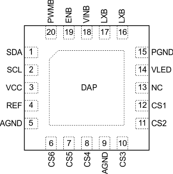
Pin Functions
| PIN | TYPE | DESCRIPTION | |
|---|---|---|---|
| NAME | NUMBER | ||
| AGND | 5, 9 | — | Signal ground of the device. |
| CS1, CS2, CS3, CS4, CS5, CS6 | 6, 7, 8, 10, 11, 12 | I | Current sink regulation inputs. They are connected to the cathode of WLEDs. The PWM loop regulates the lowest VCS to 500 mV. Each channel is limited to 30-mA current. Connect any unused CS pin to AGND or leave it open. |
| ENB | 19 | I | Enable pin |
| LXB | 16, 17 | I | Drain connection of the internal PWM switch MOSFET and external Schottky diode. |
| REF | 4 | O | The reference pin for internal error amplifier. Connect a 470-nF ceramic capacitor to REF. |
| PGND | 15 | — | Power ground of the IC. Internally, it connects to the source of the PWM switch. Tie the ground of power stage components to this ground. |
| PWMB | 20 | I | Dimming control logic input. The dimming frequency range is from 100 Hz to 25 kHz. |
| SCL | 2 | I | Clock input for I2C interface |
| SDA | 1 | I/O | Data input for I2C interface |
| VCC | 3 | I | Internal pre-regulator and supply rail for the internal logic. Do not connect any capacitor to VCC pin. |
| VINB | 18 | I | Power supply to the IC |
| VLED | 14 | I | The voltage detect pin for VOUT. |
6 Specifications
6.1 Absolute Maximum Ratings
over operating free-air temperature range (unless otherwise noted) (1)| MIN | MAX | UNIT | ||
|---|---|---|---|---|
| Voltage(2) | VINB | –0.3 | 26.4 | V |
| LXB, VLED, CS1, CS2, CS3, CS4, CS5, CS6 | –0.3 | 40 | ||
| ENB, PWMB | –0.3 | 30 | ||
| SDA, SCL, VCC | –0.3 | 3.6 | ||
| Continuous power dissipation | See Thermal Information | °C | ||
| Operating junction temperature | –40 | 150 | ||
| Storage temperature, Tstg | –65 | 150 | ||
6.2 ESD Ratings
| VALUE | UNIT | |||
|---|---|---|---|---|
| V(ESD) | Electrostatic discharge | Human-body model (HBM), per ANSI/ESDA/JEDEC JS-001(1) | ±2000 | V |
| Charged-device model (CDM), per JEDEC specification JESD22-C101(2) | ±1000 | |||
6.3 Recommended Operating Conditions
over operating free-air temperature range (unless otherwise noted)| MIN | MAX | UNIT | ||
|---|---|---|---|---|
| VIN | Input voltage | 2.5 | 24 | V |
| VOUT | Output voltage | VIN + 2 | 39 | |
| FPWM_I | PWM input signal frequency | 0.1 | 25 | kHz |
| DMIN_I | PWM input signal minimum duty cycle | 1% | ||
| FBOOST | Boost regulator switching frequency | 450 | 1200 | kHz |
| TA | Operating free-air temperature | –40 | 85 | °C |
| TJ | Operating junction temperature | –40 | 125 | |
6.4 Thermal Information
| THERMAL METRIC(1) | TPS61177A | UNIT | |
|---|---|---|---|
| RGR (VQFN) | |||
| 20 PINS | |||
| RθJA | Junction-to-ambient thermal resistance | 34.4 | °C/W |
| RθJC(top) | Junction-to-case (top) thermal resistance | 46.8 | °C/W |
| RθJB | Junction-to-board thermal resistance | 12.2 | °C/W |
| ψJT | Junction-to-top characterization parameter | 0.5 | °C/W |
| ψJB | Junction-to-board characterization parameter | 12.3 | °C/W |
| RθJC(bot) | Junction-to-case (bottom) thermal resistance | 1.0 | °C/W |
6.5 Electrical Characteristics
VINB = 12 V, PWMB/ENB = logic high, CS current = 20 mA, CS voltage = 500 mV, TA = –40°C to +85°C, typical values are at TA = 25°C (unless otherwise noted).| PARAMETER | TEST CONDITIONS | MIN | TYP | MAX | UNIT | |
|---|---|---|---|---|---|---|
| SUPPLY CURRENT | ||||||
| VINB | Input voltage range | 2.5 | 24 | V | ||
| Iq_VINB | Operating quiescent current into VIN | Device enable, no switching and no load, VINB = 12 V |
3.5 | mA | ||
| ISD | Shutdown current | VINB = 12 V, EN = low | 10 | µA | ||
| VINB = 24 V, EN = low | 15 | |||||
| VINB_UVLO | VINB undervoltage lockout threshold, voltage ramp up |
UVLO = 000 | 2.1 | 2.25 | 2.4 | V |
| UVLO = 001 | 2.4 | 2.55 | 2.7 | |||
| UVLO = 010 | 2.8 | 3 | 3.2 | |||
| UVLO = 011 | 3.3 | 3.5 | 3.7 | |||
| Other case | 3.8 | 4 | 4.2 | |||
| VIN_Hys | VIN undervoltage lockout hysteresis | 200 | mV | |||
| BOOST OUTPUT REGULATION | ||||||
| VCS | CS voltage regulation | 500 | 600 | mV | ||
| RDS(ON) | Switch FET on-resistance | VIN = 12 V | 0.20 | 0.35 | Ω | |
| VIN = 3.3 V | 0.30 | 0.40 | ||||
| ILIM | Switching MOSFET current limit | D = Dmax | 1.8 | 2.2 | 2.6 | A |
| ILEAK_LX | Switch FET leakage current | VSW = 40 V | 5 | µA | ||
| FLX | Switching frequency | FREQ = 00 | 0.36 | 0.45 | 0.54 | MHz |
| FREQ = 01 | 0.48 | 0.6 | 0.72 | |||
| FREQ = 10 | 0.64 | 0.8 | 0.96 | |||
| FREQ = 11 | 0.96 | 1.2 | 1.44 | |||
| DMAX | Maximum duty cycle | FLX = 0.8 MHz | 90% | 95% | ||
| TF | Slew rate of switching FET ON | SR = 00 | 4.6 | V/ns | ||
| SR = 01 | 3.5 | |||||
| SR = 10 | 2.5 | |||||
| SR = 11 | 1.3 | |||||
| CS CURRENT REGULATION | ||||||
| ICS | CSn current (See Figure 23) |
ICS = 0000 | 15 | mA | ||
| ICS = 0001 | 16 | |||||
| … | … | |||||
| ICS = 1111 | 30 | |||||
| ICSA | CSn current accuracy (ICSn – 20 mA × DPWM_I)/20 mA x DPWM_I |
ICS = 20 mA, MODE = 00 and 01 DPWM_I = 100%, TA = 25°C |
–3% | 3% | ||
| ICS = 20 mA, MODE = 01 DPWM_I = 255/1023, TA = 25°C |
–3% | 3% | ||||
| ICS = 20 mA, MODE = 10, DPWM_I = 255/1023, TA = 25°C |
–3% | 3% | ||||
| ICS = 20 mA, MODE = 10, DPWM_I = 51/1023, TA = 25°C |
–5% | 5% | ||||
| ICS = 20 mA, MODE = 10, DPWM_I = 10/1023, TA = 25°C |
–8% | 8% | ||||
| ICSM | Current matching (ICSn – IAVG)/IAVG | ICS = 20 mA, MODE = 00 and 01, DPWM_I = 100%, TA = 25°C |
–2% | 2% | ||
| ICS = 20 mA, MODE = 01, DPWM_I = 255/1023, TA = 25°C |
–2% | 2% | ||||
| ICS = 20 mA, MODE = 10, DPWM_I = 255/1023, TA = 25°C |
–2% | 2% | ||||
| ICS = 20 mA, MODE = 10, DPWM_I = 51/1023, TA = 25°C |
–5% | -5% | ||||
| ICS = 20 mA, MODE = 10, DPWM_I = 10/1023, TA = 25°C |
–5% | 5% | ||||
| DC dimming resolution steps | MODE = 01 and 10, FPWM_I = 0.1 to 5 kHz | 1024 | ||||
| MODE = 01 and 10, FPWM_I = 5 to 10 kHz | 512 | |||||
| MODE = 01 and 10, FPWM_I = 10 to 25 kHz | 256 | |||||
| Brightness response time | DPWM_I 10% to 90% MODE = mixed and DC, FPWM_I = 25 kHz |
400 | μs | |||
| DPWM_I 10% to 90% MODE = mixed and DC, FPWM_I = 100 Hz |
10.4 | ms | ||||
| ICSLK | CSn leakage current | VCS = 40 V | 5 | μA | ||
| ICSIR | CSn current inrush | 10% | ||||
| tMP | Minimum dimming pulse | MODE = 00 | 400 | ns | ||
| tDEG | Deglitch pulse width | 125 | ns | |||
| CONTROL AND PROTECTION | ||||||
| VH | ENB logic high threshold | VINB = 2.7 V and 3.3 V | 1.8 | V | ||
| VL | ENB logic low threshold | VINB = 2.7 V and 3.3 V | 0.5 | |||
| VH | PWMB logic high threshold | VINB = 2.7 V and 3.3 V | 1.8 | |||
| VL | PWMB logic low threshold | VINB = 2.7 V and 3.3 V | 0.5 | |||
| RPD | Pulldown resistor on ENB | ENB = 3.3 V | 300 | 600 | 1200 | kΩ |
| Pulldown resistor on PWMB | PWMB = 3.3 V | 300 | 600 | 1200 | ||
| VOVP | Output overvoltage threshold | 39 | 39.5 | 40 | V | |
| Tshutdown | Thermal shutdown threshold | 150 | °C | |||
| Thermal shutdown hysteresis | 15 | |||||
| FSAMPLE | Input sampling oscillator frequency | 22 | 25 | 29 | MHz | |
6.6 I2C Timing Requirements
| MIN | NOM | MAX | UNIT | |||
|---|---|---|---|---|---|---|
| ADDR | Configuration parameters slave address | Write | 58h | |||
| Read | 59h | |||||
| VIL | Low level input voltage | Supply = 2.5 V, VIN falling, standard and fast modes |
0.75 | V | ||
| VIH | High level input voltage | Supply = 2.5 V, VIN rising, standard and fast modes |
1.75 | V | ||
| VHYS | Hysteresis | Supply = 2.5 V, applicable to fast mode only |
125 | mV | ||
| VOL | Low level output voltage | Sinking 3 mA | 500 | mV | ||
| CI | Input capacitance | 10 | pF | |||
| ƒSCL | Clock frequency | Standard mode | 100 | kHz | ||
| Fast mode | 400 | |||||
| tLOW | Clock low period | Standard mode | 4.7 | µs | ||
| Fast mode | 1.3 | |||||
| tHIGH | Clock high period | Standard mode | 4 | µs | ||
| Fast mode | 0.6 | |||||
| tBUF | Bus free time between a STOP and a START condition | Standard mode | 4.7 | µs | ||
| Fast mode | 1.3 | |||||
| thd:STA | Hold time for a repeated START condition | Standard mode | 4 | µs | ||
| Fast mode | 0.6 | |||||
| tsu:STA | Set-up time for a repeated START condition | Standard mode | 4 | µs | ||
| Fast mode | 0.6 | |||||
| tsu:DAT | Data set-up time | Standard mode | 250 | ns | ||
| Fast mode | 100 | |||||
| thd:DAT | Data hold time | Standard mode | 0.05 | 3.45 | µs | |
| Fast mode | 0.05 | 0.9 | ||||
| tRCL1 | Rise time of SCL after a repeated START condition and after an ACK bit | Standard mode | 20+0.1CB | 1000 | ns | |
| Fast mode | 20+0.1CB | 1000 | ||||
| tRCL | Rise time of SCL | Standard mode | 20+0.1CB | 1000 | ns | |
| Fast mode | 20+0.1CB | 300 | ||||
| tFCL | Fall time of SCL | Standard mode | 20+0.1CB | 300 | ns | |
| Fast mode | 20+0.1CB | 300 | ||||
| tRDA | Rise time of SDA | Standard mode | 20+0.1CB | 1000 | ns | |
| Fast mode | 20+0.1CB | 300 | ||||
| tFDA | Fall time of SDA | Standard mode | 20+0.1CB | 300 | ns | |
| Fast mode | 20+0.1CB | 300 | ||||
| tsu:STO | Set-up time for STOP condition | Standard mode | 4 | µs | ||
| Fast mode | 0.6 | |||||
| CB | Capacitive load on SDA and SCL | Standard mode | 400 | pF | ||
| Fast mode | 400 | |||||
| NWRITE | Number of write cycles | 1000 | ||||
| tWRITE | Write time | 100 | ms | |||
| Data retention | Storage temperature = 150°C | 100,000 | hrs | |||
6.7 Typical Characteristics
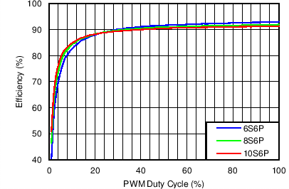
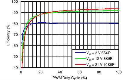
Table 1. Table of Graphs
| TITLE | DESCRIPTION | FIGURE |
|---|---|---|
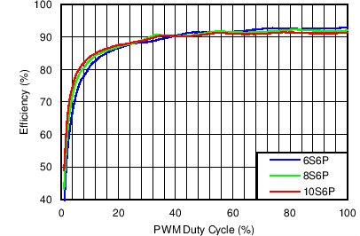
| Efficiency vs PWM Duty in PWM Mode | VIN = 12 V, VOUT = 6S6P, 8S6P, 10S6P, ICS = 20 mA, L = 10 µH | Figure 1 |
| Efficiency vs PWM Duty in PWM Mode | VIN = 3 V, 12 V, 21 V, VOUT = 6S6P, 8S6P, 10S6P, L = 10 µH | Figure 2 |
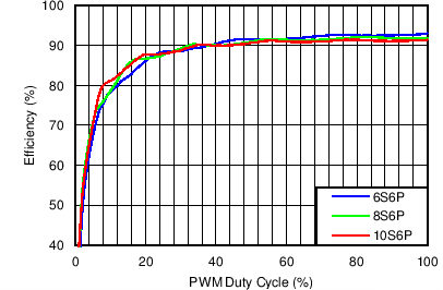
| Efficiency vs PWM duty in Mixed Mode | VIN = 12 V, VOUT = 6S6P, 8S6P, 10S6P, ICS = 20 mA, L = 10 µH | Figure 3 |
| Efficiency vs PWM duty in Mixed Mode | VIN = 3 V, 12 V, 21 V, VOUT = 6S6P, 8S6P, 10S6P, L = 10 µH | Figure 4 |
| Efficiency vs PWM duty in Analog Mode | VIN = 12 V, VOUT = 6S6P, 8S6P, 10S6P, ICS = 20 mA, L = 10 µH | Figure 5 |
| Efficiency vs PWM duty in Analog Mode | VIN = 3 V, 12 V, 21 V, VOUT = 6S6P, 8S6P, 10S6P, L = 10 µH | Figure 6 |
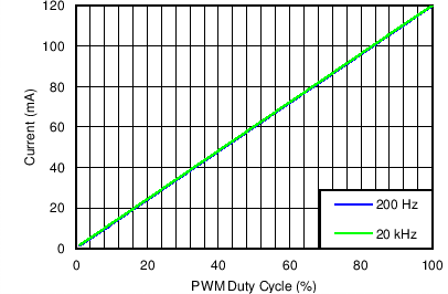
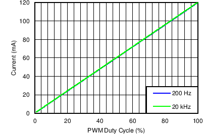
| Dimming Linearity in PWM Mode | VIN = 12 V, VOUT = 10S6P , FDIM = 200 Hz and 20 kHz, L = 10 µH | Figure 7 |
| Dimming Linearity in Mixed Mode | VIN = 12 V, VOUT = 10S6P , FDIM = 200 Hz and 20 kHz, L = 10 µH | Figure 8 |
| Dimming linearity in Analog Mode | VIN = 12 V, VOUT = 10S6P , FDIM = 200 Hz and 20 kHz, L = 10 µH | Figure 9 |
| Switch Waveform | VIN = 3 V, VOUT = 6S6P, Duty = 100%, L = 10 µH | Figure 10 |
| Switch Waveform | VIN = 12 V, VOUT = 10S6P, Duty = 100%, L = 10 µH | Figure 11 |
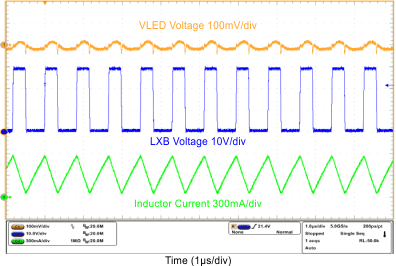
| Mixed-Mode Dimming Ripple | VIN = 12 V, VOUT = 10S6P, FDIM = 200 Hz, Duty = 50%, L = 10 µH | Figure 12 |
| Mixed-Mode Dimming Ripple | VIN = 12 V, VOUT = 10S6P, FDIM = 200 Hz, Duty = 12.5%, L = 10 µH | Figure 13 |
| Mixed-Mode Dimming Ripple | VIN = 12 V, VOUT = 10S6P, FDIM = 20 kHz, Duty = 12.5%, L = 10 µH | Figure 14 |
| PWM-Mode Dimming Ripple | VIN = 12 V, VOUT = 10S6P, FDIM = 200 Hz, Duty = 50%, L = 10 µH | Figure 15 |
| PWM-Mode Dimming Ripple | VIN = 12 V, VOUT = 10S6P, FDIM = 20 kHz, Duty = 50%, L = 10 µH | Figure 16 |

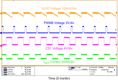
| FDIM = 200 Hz | Duty = 12.5% | |
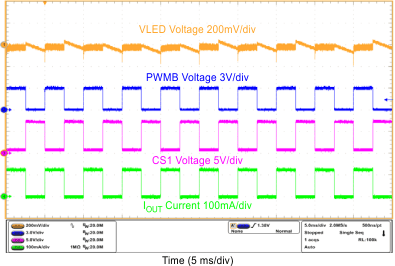
| FDIM = 200 Hz | Duty = 50% | |
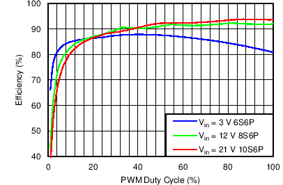
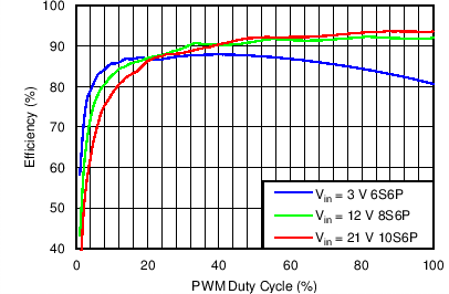
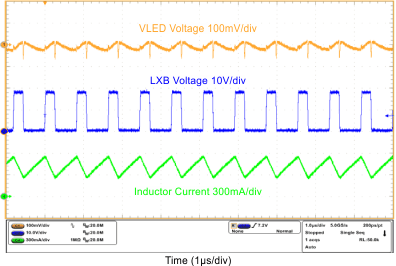
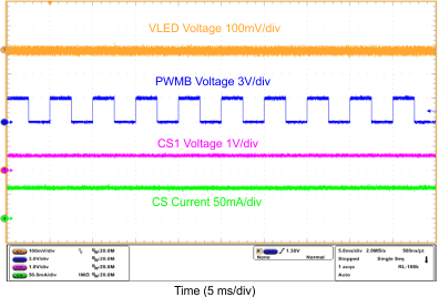
| FDIM = 200 Hz | Duty = 50% | |
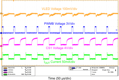
| FDIM = 20 kHz | Duty = 12.5% | |
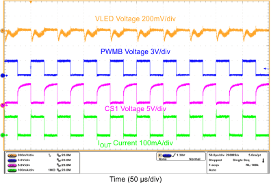
| FDIM = 20 kHz | Duty = 50% | |
7 Detailed Description
7.1 Overview
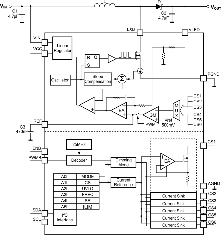
The TPS61177A is a high-efficiency, high output voltage white-LED (WLED) driver for notebook panel backlighting applications. Due to the large number of white LEDs required to provide backlighting for medium-to-large display panels, the LEDs must be arranged in parallel strings of several LEDs in series. Therefore, the backlight driver for battery-powered systems is almost always a boost regulator with multiple current-sink regulators. Having more WLEDs in series reduces the number of parallel strings, thus improving overall current matching. However, the efficiency of the boost regulator declines due to the need for high output voltage. Also, there must be enough white LEDs in series to ensure the output voltage stays above the input voltage range.
The TPS61177A device has integrated all of the key function blocks to power and control up to 72 WLEDs. The device includes a 1.8-A, 40-V boost regulator, six 30-mA current sink regulators, and a protection circuit for overcurrent, overvoltage, open LED, short LED, and overtemperature failures. The TPS61177A integrates mixed mode dimming methods with the PWM interface to reduce the output ripple voltage and audible noise. Optional direct PWM and pure analog dimming modes are user selectable through the I2C programming.
7.2 Functional Block Diagram
7.3 Feature Description
7.3.1 Supply Voltage
The TPS61177A device has a built-in linear regulator to supply the device analog and logic circuit. The VCC pin is recommended to be open without any capacitance load. VCC does not have high current sourcing capability for external use and typically is regulated at 3.3 V.
7.3.2 Boost Regulator
The fixed-frequency PWM boost converter uses current-mode control and has integrated loop compensation. The internal compensation ensures stable output over the full input and output voltage ranges assuming the recommended inductance and output capacitance values shown in Figure 36. The output voltage of the boost regulator is automatically set by the device to minimize voltage drop across the CS pins. The device regulates the lowest CS pin to 500 mV at 20-mA current and consistently adjusts the boost output voltage to account for any changes in LED forward voltages. If the input voltage is higher than the sum of the WLED forward voltage drops (at low duty cycles), the boost converter is not able to regulate the output due to its minimum duty cycle limitation. In this case, increase the number of WLEDs in series or include series ballast resistors in order to provide enough headroom for the converter to boost the output voltage. Since the TPS61177A integrates a 1.8-A, 40-V power MOSFET, the boost converter can provide up to a 39-V output voltage.
7.3.3 Programmable Switch Frequency and Slew Rate
Both switching frequency and slew rate of TPS61177A can be programmable by a E2PROM register value which is pre-set before device power up. The switching frequency has four options adjustable to 450 kHz, 600 kHz, 800 kHz, or 1200 kHz. The slew rate of switching FET from off to on also has four selections: 1.3 V/ns, 2.5 V/ns, 3.5 V/ns to 4.6 V/ns.
See FREQ (A3h) and SR (A4h) for E2PROM address and data table of boost switching frequency programming and boost switching slew rate selection.
The adjustable switching frequency feature provides the user with the flexibility of choosing either a faster switching frequency by using an inductor with smaller inductance and footprint or a slower switching frequency to get potentially higher efficiency due to lower switching losses. In additional, the selectable slew rate for switching gives flexibility to trade off between switching loss and electronic-magnetic interference (EMI) effects to the application system.
7.3.4 LED Current Sinks
The six current sink regulators embedded in the TPS61177A can be collectively configured to provide up to a maximum of 30 mA each. These six specialized current sinks are accurate to within ±3% max for currents at 20 mA, with a string-to-string difference of ±2%.
Each CS channel current must be programmed to the highest WLED current expected; each CS channel current is programmable from 15 mA to 30 mA by an E2PROM register through the I2C interface. See CS (A1h) for the E2PROM register table of CS current programming.
7.3.5 Enable and Start-Up Timing
The internal regulator which provides VCC wakes up as soon as ENB is applied. VCC does not come to full regulation until VINB voltage is above UVLO. Before boost convert start-up, the TPS61177A checks the status of all current feedback channels and shuts down any unused feedback channels. It is recommended to short the unused channels to ground for faster start-up.
After the device is enabled, if the PWM pin is left floating or grounded, the output voltage of the TPS61177A regulates to the minimum output voltage. Once the device detects a voltage on the PWM pin, the TPS61177A begins to regulate the CS pin current, as a pre-set per the E2PROM register data, according to the duty cycle of the signal on the PWMB pin. The boost converter output voltage rises to the appropriate level to accommodate the sum of the white LED string with the highest forward voltage drops plus the headroom of the current sink at that current.
Pulling the ENB pin low shuts down the device, resulting in consumption of less than 10 µA in shutdown mode.
The TPS61177A also integrates power-up sequence control for start-up. There is no specified power or control signal sequence requirement for VINB, ENB, and PWMB. Figure 17 provides the detail timing diagram for TPS61177A start-up and shutdown.
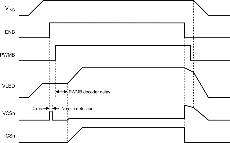 Figure 17. Start-up and Shutdown Timing Diagram
The PWMB decoder delay time period is determined by different dimming mode, input duty cycle, and frequency on the PWMB pin. In PWM mode, the decoder delay time is zero. Once the rising edge is detected on the PWMB pin, the output voltage starts ramping up immediately. While in mixed dimming mode or analogdimming mode, the decoder delay time is equal to twice input PWM signal cycle time and 400 µs minimally. If PWM signal input keeps at high level after first rising edge, the decoder delay is about 20 ms.
Figure 18 provides the detail timing diagram for TPS61177A start-up and shutdown when one of CS channel is open. The VLED voltage always ramps up to the overvoltage protection threshold which is 39.5 V typically, if one of CS pin is floating. The device then detects the zero current string, and removes it from the feedback loop.
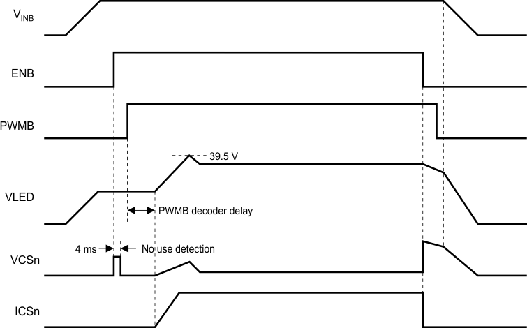 Figure 18. Start-Up and Shutdown Timing Diagram (Mixed Mode and DC Mode)
7.3.6 Input Undervoltage Protection (UVLO)
The TPS61177A will not start up until the VINB voltage is higher than the UVLO threshold which is preset by E2PROM register data. During normal operation, if the VINB drops below UVLO with 200-mV hysteresis, the TPS61177A immediately shuts down. See UVLO (A2h) for E2PROM address and data table of UVLO threshold.
7.3.7 Overvoltage Protection (OVP)
The TPS61177A integrates output OVP which is fixed at 39.5 V typically. Once the VLED pin detects the voltage higher than 39.5 V, the boost switching regulator stops switching until the voltage of VLED pin drop below 39.5 V with 500-mV hysteresis.
7.3.8 Current-Sink Open Protection
If one of the device WLED strings is open, the device automatically detects and disables that string. The open WLED string is detected by sensing no current in the corresponding CS pin. As a result, the TPS61177A deactivates the open current sink and removes it from the voltage feedback loop. Subsequently, the output voltage drops and is regulated to the minimum voltage required for the connected WLED strings. The CS currents of the connected WLED strings remain in regulation.
The device turns off if it detects that all of the WLED strings are open. If an open string is reconnected again, a power-on reset (POR) or ENB pin toggling is required to reactivate a previously deactivated string.
7.3.9 Overcurrent Protection
The TPS61177A has a pulse-by-pulse overcurrent limit of 1.8 A (minimum). The PWM switch turns off when the inductor current reaches this current threshold. The PWM switch remains off until the beginning of the next switching cycle. This protects the device and external components during an overload condition. When there is a sustained overcurrent condition more than 2 ms, the device shuts down and requires a POR or EN pin toggling to restart. The overcurrent shutdown protection can be disabled by E2PROM register through I2C interface. See ILIM (A5h) for E2PROM register table of ILIM shutdown protection programming.
7.3.10 Thermal Protection
When the junction temperature of the TPS61177A is over 150°C, the thermal protection circuit is triggered and shuts down the device immediately. The device automatically restarts when the junction temperature is back to less than 150°C with about 15°C hysteresis.
7.4 Device Functional Modes
7.4.1 Mode Selection
The mixed-mode dimming method, analog dimming method, or direct PWM dimming method can be selected through the E2PROM register. See MODE (A0h) for E2PROM register table of dimming mode programming.
7.4.2 Analog and PWM Mixed Dimming Mode
In analog and PWM mixed mode, the TPS61177A features both analog dimming and PWM digital dimming. Analog dimming can provide potentially a lower power requirement for the same WLED brightness output because of a low voltage drop across each WLED when the current is low. Digital PWM dimming provides less WLED color distortion since the WLED current is held at 25% of full scale when the WLED is on.
The brightness control signal on the PWM pin is translated to a 10-bit digital signal and sent to control the six current regulators. Each current regulator outputs is DC, and PWM (25% < DPWM < 100%) modulates the amplitude of the currents from 25% to 100% of preset full-scale current. For DPWM < 25%, each CS turns on/off at translated duty cycle and same frequency to the input PWM, and in the WLED on duty current is regulated at 25% of full scale. Mixed-mode dimming provides the benefits of both the analog and PWM dimming. For 25% < DPWM < 100%, analog dimming benefits the low power requirement and increases the power to brightness transform efficiency. At light load conditions, DPWM < 25%, the PWM dimming provides both high accuracy brightness and low color distortion. Figure 19 provides the detailed timing diagram of the analog and PWM mixed dimming mode.
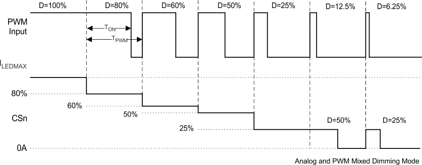 Figure 19. Analog and PWM Mixed-Mode Dimming Diagram
7.4.3 Analog Dimming Mode
In analog dimming mode, TPS61177A features pure analog dimming all over the brightness range of full-scale LED current. Analog dimming can provide potentially low power requirement for same WLED brightness output because of low voltage drop across each WLED when the current is low. In additional, the brightness control signal on the PWMB pin is translated to an up to 10-bits digital signal and sent to control the six current regulators. Each current regulator output DC modulates the amplitude of the currents from 1% to 100% of preset full-scale current. Figure 20 provides the detailed timing diagram of the analog dimming mode.
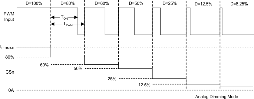 Figure 20. Analog-Mode Dimming Diagram
7.4.4 Direct PWM Dimming
In direct PWM mode, all current feedback channels are turned on and off and are synchronized with the input PWM signal. Figure 21 provides the detailed timing diagram of the direct PWM dimming mode.
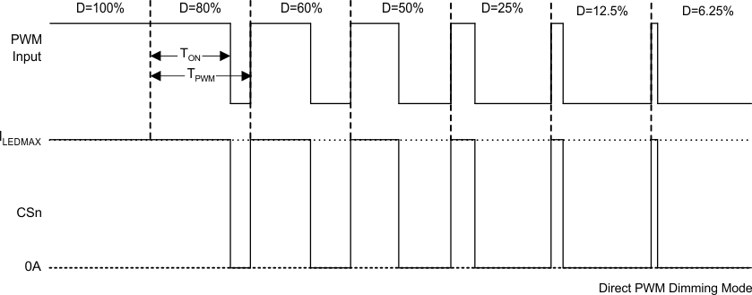 Figure 21. Direct PWM-Mode Dimming Diagram
7.5 Programming
7.5.1 Configuration Parameters
Table 2 shows the memory map of the configuration parameters.
Table 2. Configuration Memory Map
| REGISTER ADDRESS | REGISTER NAME | FACTORY DEFAULT | DESCRIPTION |
|---|---|---|---|
| A0h | MODE | 01h | Sets brightness dimming mode |
| A1h | CS | 05h | Sets the current sinks full scale current |
| A2h | UVLO | 03h | Sets the input voltage UVLO threshold |
| A3h | FREQ | 01h | Sets the boost switching frequency |
| A4h | SR | 00h | Sets the boost switching slew rate |
| A5h | ILIM | 00h | Enables/disables the shutdown protection for current limit |
| FFh | Control | 00h | Controls whether read and write operations access RAM or E2PROM registers. |
7.6 Register Maps
7.6.1 MODE (A0h)
The MODE register can be written to and read from.
| 7 | 6 | 5 | 4 | 3 | 2 | 1 | 0 |
| RESERVED | MODE | ||||||
| R/W-0 | R/W-1 | ||||||
| LEGEND: R/W = Read/Write; R = Read only; -n = value after reset |
Table 3. MODE Register Bit Field Descriptions
| Bit | Field | Type | Reset | Description |
|---|---|---|---|---|
| 7:2 | RESERVED | R/W | 0 | These bits are reserved for future use. During write operations, data intended for these bits are ignored, and during read operations 0 is returned. |
| 1:0 | MODE | R/W | 1 | These bits configure the current sink dimming method for brightness control. 00 = Direct PWM dimming mode 01 = Analog and PWM mixed dimming mode 10 = Analog dimming mode |
7.6.2 CS (A1h)
The CS register can be written to and read from.
| 7 | 6 | 5 | 4 | 3 | 2 | 1 | 0 |
| RESERVED | CS | ||||||
| R/W-0 | R/W-5 | ||||||
| LEGEND: R/W = Read/Write; R = Read only; -n = value after reset |
Table 4. CS Register Bit Descriptions
| Bit | Field | Type | Reset | Description | |
|---|---|---|---|---|---|
| 7:4 | RESERVED | R/W | 0 | These bits are reserved for future use. During write operations, data intended for these bits are ignored, and during read operations 0 is returned. | |
| 3:0 | CS | R/W | 5 | These bits select the full scale current for all six current sinks. | |
| 0000: ICS = 15 mA 0001: ICS = 16 mA 0010: ICS = 17 mA 0011: ICS = 18 mA 0100: ICS = 19 mA 0101: ICS = 20 mA 0110: ICS = 21 mA 0111: ICS = 22 mA |
1000: ICS = 23 mA 1001: ICS = 24 mA 1010: ICS = 25 mA 1011: ICS = 26 mA 1100: ICS = 27 mA 1101: ICS = 28 mA 1110: ICS = 29 mA 1111: ICS = 30 mA |
||||
7.6.3 UVLO (A2h)
The UVLO register can be written to and read from.
| 7 | 6 | 5 | 4 | 3 | 2 | 1 | 0 |
| RESERVED | UVLO | ||||||
| R/W-0 | R/W-3 | ||||||
| LEGEND: R/W = Read/Write; R = Read only; -n = value after reset |
Table 5. UVLO Register Bit Field Descriptions
| Bit | Field | Type | Reset | Description |
|---|---|---|---|---|
| 7:3 | RESERVED | R/W | 0 | These bits are reserved for future use. During write operations data intended for these bits is ignored, and during read operations 0 is returned. |
| 2:0 | UVLO | R/W | 3 | These bits select the UVLO threshold. 000: VUVLO = 2.25 V 001: VUVLO = 2.55 V 010: VUVLO = 3 V 011: VUVLO = 3.5 V 100: VUVLO = 4 V Others: VUVLO = 4 V |
7.6.4 FREQ (A3h)
The FREQ register can be written to and read from.
| 7 | 6 | 5 | 4 | 3 | 2 | 1 | 0 |
| RESERVED | FREQ | ||||||
| R/W-0 | R/W-1 | ||||||
| LEGEND: R/W = Read/Write; R = Read only; -n = value after reset |
Table 6. FREQ Register Bit Field Descriptions
| Bit | Field | Type | Reset | Description |
|---|---|---|---|---|
| 7:2 | RESERVED | R/W | 0 | These bits are reserved for future use. During write operations, data intended for these bits are ignored, and during read operations 0 is returned. |
| 1:0 | FREQ | R/W | 1 | These bits configure the switching frequency. 00: FLX = 450 kHz 01: FLX = 600 kHz 10: FLX = 800 kHz 11: FLX = 1200 kHz |
7.6.5 SR (A4h)
The SR register can be written to and read from.
| 7 | 6 | 5 | 4 | 3 | 2 | 1 | 0 |
| RESERVED | SR | ||||||
| R/W-0 | R/W-0 | ||||||
| LEGEND: R/W = Read/Write; R = Read only; -n = value after reset |
Table 7. SR Register Bit Field Descriptions
| Bit | Field | Type | Reset | Description |
|---|---|---|---|---|
| 7:2 | RESERVED | R/W | 0 | These bits are reserved for future use. During write operations, data intended for these bits are ignored, and during read operations 0 is returned. |
| 1:0 | SR | R/W | 0 | These bits configure the falling slew rate of switching voltage from OFF to ON. 00: SR = 4.6 V/ns 01: SR = 3.5 V/ns 10: SR = 2.5 V/ns 11: SR = 1.3 V/ns |
7.6.6 ILIM (A5h)
The ILIM register can be written to and read from.
| 7 | 6 | 5 | 4 | 3 | 2 | 1 | 0 |
| RESERVED | ILIM | ||||||
| R/W-0 | R/W-0 | ||||||
| LEGEND: R/W = Read/Write; R = Read only; -n = value after reset |
Table 8. ILIM Register Bit Field Descriptions
| Bit | Field | Type | Reset | Description |
|---|---|---|---|---|
| 7:1 | RESERVED | R/W | 0 | These bits are reserved for future use. During write operations, data intended for these bits are ignored, and during read operations 0 is returned. |
| 0 | ILIM | R/W | 0 | This bit configures the current limit shutdown protection. 0 = Disable current limit shutdown protection 1 = Enable current limit shutdown protection |
7.6.7 Control (FFh)
| 7 | 6 | 5 | 4 | 3 | 2 | 1 | 0 |
| WED | RESERVED | RED | |||||
| R/W-0 | R/W-0 | ||||||
| LEGEND: R/W = Read/Write; R = Read only; -n = value after reset |
Table 9. Control Register Bit Field Descriptions
| Bit | Field | Type | Reset | Description |
|---|---|---|---|---|
| 7 | WED | Setting this bit forces the contents of all registers to be copied into E2PROM, thereby making them the default values during power up. When the contents of all the registers have been written to E2PROM, the TPS61177A device automatically resets this bit. |
||
| 6:1 | RESERVED | R/W | 0 | These bits are reserved for future use. During write operations, data intended for these bits are ignored, and during read operations 0 is returned. |
| 0 | RED | R/W | 0 | The state of this bit determines whether read operations return the contents of the registers or the contents of the E2PROM. 0 = Read operations return the contents of the registers. 1 = Read operations return the contents of the E2PROM. |
7.6.8 Example – Writing to a Single RAM Register
- Bus master sends START condition
- Bus master sends 7-bit slave address plus low R/W bit (58h)
- TPS61177A acknowledges
- Bus master sends address of RAM register (A0h)
- TPS61177A acknowledges
- Bus master sends data to be written
- TPS61177A acknowledges
- Bus master sends STOP condition
 Figure 29. Writing To A Single Ram Register
7.6.9 Example – Writing to Multiple RAM Registers
- Bus master sends START condition
- Bus master sends 7-bit slave address plus low R/W bit (58h).
- TPS61177A acknowledges
- Bus master sends address of first RAM register to be written to (A0h)
- TPS61177A acknowledges
- Bus master sends data to be written to first RAM register
- TPS61177A acknowledges
- Bus master sends data to be written to RAM register at next higher address (auto-increment)
- TPS61177A acknowledges
- Steps (8) and (9) repeated until data for final RAM register has been sent
- TPS61177A acknowledges
- Bus master sends STOP condition
 Figure 30. Writing To Multiple Ram Registers
7.6.10 Example – Saving Contents of all RAM Registers to E2PROM
- Pull high the Enable pin of TPS61177A
- Pull the PWM pin of TPS61177A to low
- Bus master sends START condition
- Bus master sends 7-bit slave address plus low R/W bit (58h)
- TPS61177A acknowledges
- Bus master sends address of Control Register (FFh)
- TPS61177A acknowledges
- Bus master sends data to be written to the Control Register (80h)
- TPS61177A acknowledges
- Bus master sends STOP condition
 Figure 31. Saving Contents Of All Ram Registers To E2PROM
The TPS61177A needs a 50-ms time period after receiving STOP condition for saving all RAM registers data to E2PROM. If bus master send 7-bit slave address to call TPS61177A again within 50-ms period, the TPS61177A pulls down the SCL line to LOW until the all RAM registers data saving to E2PROM is completed.
7.6.11 Example – Reading from a Single RAM Register
- Bus master sends START condition
- Bus master sends 7-bit slave address plus low R/W bit (58h)
- TPS61177A acknowledges
- Bus master sends address of Control Register (FFh)
- TPS61177A acknowledges
- Bus master sends data for Control Register (00h)
- TPS61177A acknowledges
- Bus master sends STOP condition
- Bus master sends START condition
- Bus master sends 7-bit slave address plus low R/W bit (58h)
- TPS61177A acknowledges
- Bus master sends address of RAM register (A0h)
- TPS61177A acknowledges
- Bus master sends REPEATED START condition
- Bus master sends 7-bit slave address plus high R/W bit (59h)
- TPS61177A acknowledges
- TPS61177A sends RAM register data
- Bus master not acknowledges
- Bus master sends STOP condition
 Figure 32. Reading From A Single Ram Register
7.6.12 Example – Reading from a Single E2PROM Register
- Bus master sends START condition
- Bus master sends 7-bit slave address plus low R/W bit (58h)
- TPS61177A acknowledges
- Bus master sends address of Control Register (FFh)
- TPS61177A acknowledges
- Bus master sends data for Control Register (01h)
- TPS61177A acknowledges
- Bus master sends STOP condition
- Bus master sends START condition
- Bus master sends 7-bit slave address plus low R/W bit (58h)
- TPS61177A acknowledges
- Bus master sends address of RAM register (A0h)
- TPS61177A acknowledges
- Bus master sends REPEATED START condition
- Bus master sends 7-bit slave address plus high R/W bit (59h)
- TPS61177A acknowledges
- TPS61177A sends E2PROM register data
- Bus master not acknowledges
- Bus master sends STOP condition
 Figure 33. Reading From A Single E2PROM Register
7.6.13 Example – Reading from Multiple RAM Registers
- Bus master sends START condition
- Bus master sends 7-bit slave address plus low R/W bit (58h)
- TPS61177A acknowledges
- Bus master sends address of Control Register (FFh)
- TPS61177A acknowledges
- Bus master sends data for Control Register (00h)
- TPS61177A acknowledges
- Bus master sends STOP condition
- Bus master sends START condition
- Bus master sends 7-bit slave address plus low R/W bit (58h)
- TPS61177A acknowledges
- Bus master sends address of RAM register (A0h)
- TPS61177A acknowledges
- Bus master sends REPEATED START condition
- Bus master sends 7-bit slave address plus high R/W bit (59h)
- TPS61177A acknowledges
- TPS61177A sends contents of first RAM register to be read
- Bus master acknowledges
- TPS61177A sends contents of second RAM register to be read
- Bus master acknowledges
- TPS61177A sends contents of third (last) RAM register to be read
- Bus master not acknowledges
- Bus master sends STOP condition
 Figure 34. Reading From A Multiple Ram Register
7.6.14 Example – Reading from Multiple E2PROM Registers
- Bus master sends START condition
- Bus master sends 7-bit slave address plus low R/W bit (58h)
- TPS61177A acknowledges
- Bus master sends address of Control Register (FFh)
- TPS61177A acknowledges
- Bus master sends data for Control Register (01h)
- TPS61177A acknowledges
- Bus master sends STOP condition
- Bus master sends START condition
- Bus master sends 7-bit slave address plus low R/W bit (58h)
- TPS61177A acknowledges
- Bus master sends address of E2PROM register (00h)
- TPS61177A acknowledges
- Bus master sends REPEATED START condition
- Bus master sends 7-bit slave address plus high R/W bit (59h)
- TPS61177A acknowledges
- TPS61177A sends contents of first E2PROM register to be read
- Bus master acknowledges
- TPS61177A sends contents of second E2PROM register to be read
- Bus master acknowledges
- TPS61177A sends contents of third (last) E2PROM register to be read
- Bus master not acknowledges
- Bus master sends STOP condition
 Figure 35. Reading From Multiple E2PROM Registers