SNVSA85C October   2015  – January 2017 LM27761

PRODUCTION DATA.  

  1. Features
  2. Applications
  3. Description
    1.     Device Images
      1.      Typical Application
  4. Revision History
  5. Pin Configuration and Functions
    1.     Pin Functions
  6. Specifications
    1. 6.1 Absolute Maximum Ratings
    2. 6.2 ESD Ratings
    3. 6.3 Recommended Operating Conditions
    4. 6.4 Thermal Information
    5. 6.5 Electrical Characteristics
    6. 6.6 Typical Characteristics
  7. Detailed Description
    1. 7.1 Overview
    2. 7.2 Functional Block Diagram
    3. 7.3 Feature Description
      1. 7.3.1 Undervoltage Lockout
      2. 7.3.2 Input Current Limit
      3. 7.3.3 PFM Operation
      4. 7.3.4 Output Discharge
      5. 7.3.5 Thermal Shutdown
    4. 7.4 Device Functional Modes
      1. 7.4.1 Shutdown Mode
      2. 7.4.2 Enable Mode
  8. Application and Implementation
    1. 8.1 Application Information
    2. 8.2 Typical Application - Regulated Voltage Inverter
      1. 8.2.1 Design Requirements
      2. 8.2.2 Detailed Design Procedure
        1. 8.2.2.1 Custom Design With WEBENCH® Tools
        2. 8.2.2.2 Charge-Pump Voltage Inverter
        3. 8.2.2.3 Negative Low-Dropout Linear Regulator
        4. 8.2.2.4 Power Dissipation
        5. 8.2.2.5 Output Voltage Setting
        6. 8.2.2.6 External Capacitor Selection
          1. 8.2.2.6.1 Charge-Pump Output Capacitor
          2. 8.2.2.6.2 Input Capacitor
          3. 8.2.2.6.3 Flying Capacitor
          4. 8.2.2.6.4 LDO Output Capacitor
      3. 8.2.3 Application Curves
  9. Power Supply Recommendations
  10. 10Layout
    1. 10.1 Layout Guidelines
    2. 10.2 Layout Example
  11. 11Device and Documentation Support
    1. 11.1 Device Support
      1. 11.1.1 Development Support
        1. 11.1.1.1 Custom Design With WEBENCH® Tools
    2. 11.2 Receiving Notification of Documentation Updates
    3. 11.3 Community Resources
    4. 11.4 Trademarks
    5. 11.5 Electrostatic Discharge Caution
    6. 11.6 Glossary
  12. 12Mechanical, Packaging, and Orderable Information

Application Curves

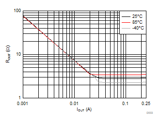
LM27761 D003_SNVSA85.gif
VIN = 3 V VOUT = –1.8 V
Figure 18. Charge-Pump Output Impedance vs
Output Current
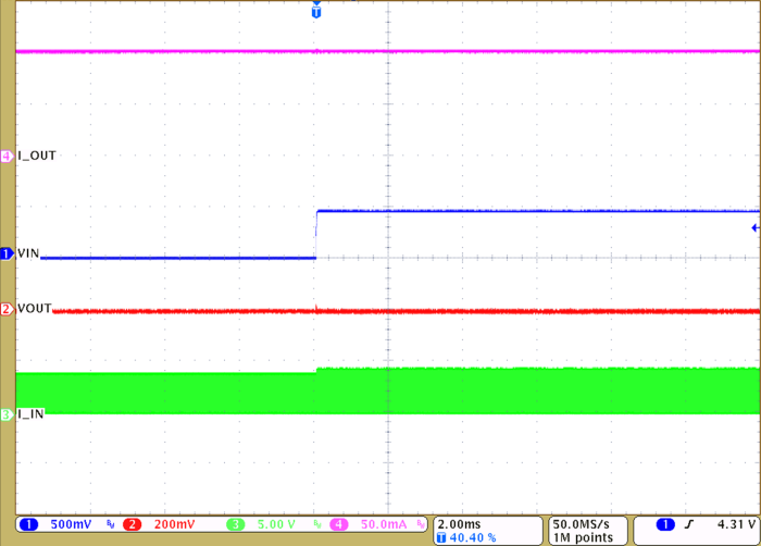
LM27761 wvfrm05_line_step_snvsa85.png
VIN = 4V to 4.5 V VOUT = –1.8 V IOUT = 100 mA
Figure 20. Line Step
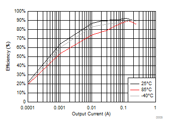
LM27761 D005_SNVSA85.gif
VIN = 5.5 V VOUT = –5 V R1 = 1.54 MΩ R2 = 500 kΩ
Figure 22. Efficiency vs Output Current
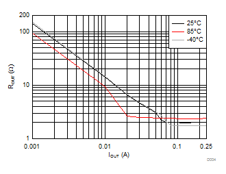
LM27761 D004_SNVSA85.gif
VIN = 5.5 V VOUT = –5 V
Figure 19. Charge-Pump Output Impedance vs
Output Current
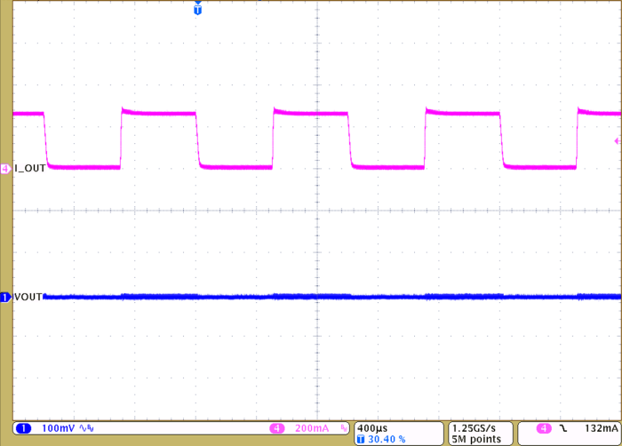
LM27761 wvfrm06_load_step_snvsa85.png
VIN = 3 V VOUT = –1.8 V
Figure 21. Load Step