SNVU792 September 2021 LM5152-Q1
5 PCB Layers
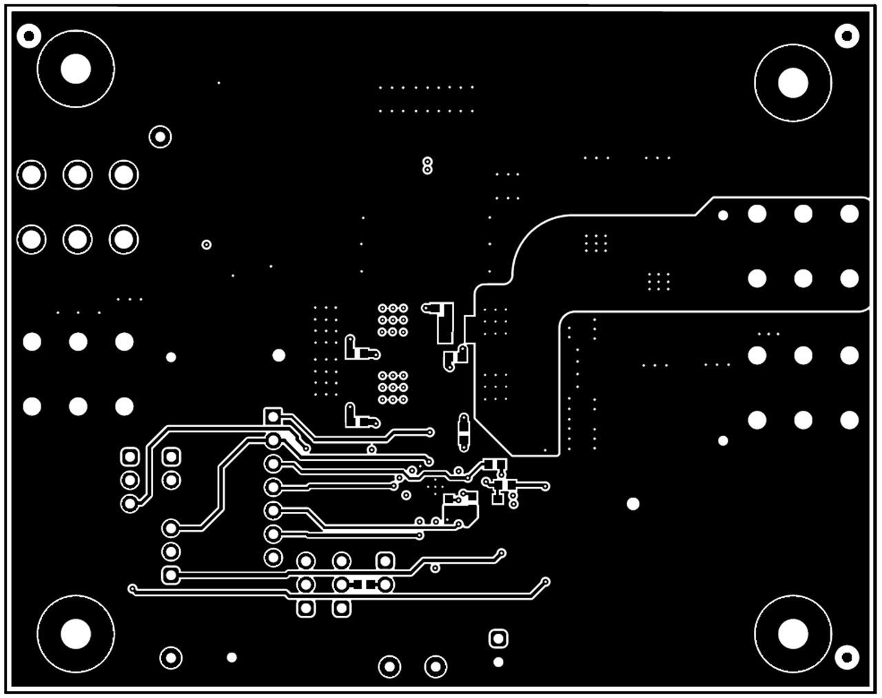
Figure 5-1 through Figure 5-6 illustrate the EVM PCB layout.
 Figure 5-1 Layout: Top Silk Screen
 Figure 5-3 Layout: Signal Layer 1
 Figure 5-5 Layout: Bottom Layer
 Figure 5-2 Layout: Top Layer
 Figure 5-4 Layout: Signal Layer 2
 Figure 5-6 Layout: Bottom Silk Screen