SNVU793 September 2021 LM5158
6.2 Output Regulation
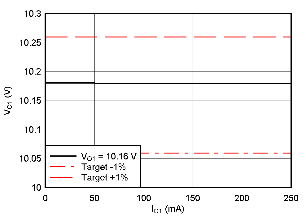
 Figure 6-2 Main Output Voltage Regulation
Versus Main Output Load (Io2, Io3, Io4 = 10%)
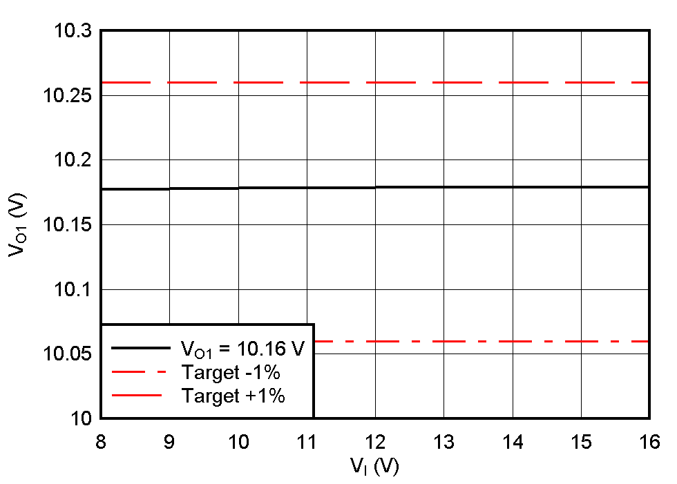
 Figure 6-4 Main Output Voltage Regulation
Versus Input Voltage (Io2, Io3, Io4 = 100%)
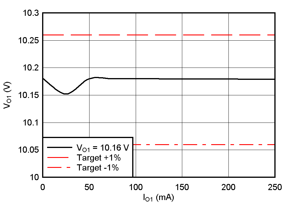
 Figure 6-3 Main Output Voltage Regulation
Versus Main Output Load (Io2, Io3, Io4 = 100%)
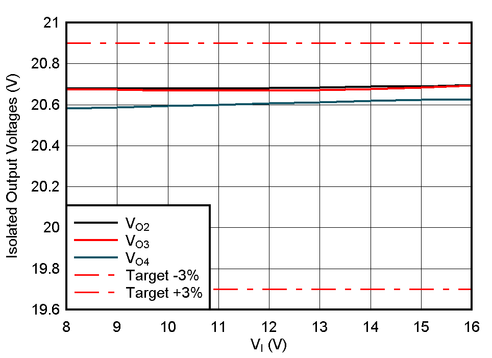
 Figure 6-5 Voltage Regulation of Isolated
Outputs Versus Input Voltage at 10% load