SNVU818 May 2022 TPS62901-Q1 , TPS62902-Q1 , TPS62903-Q1
1.2.6 Loop Response Measurement
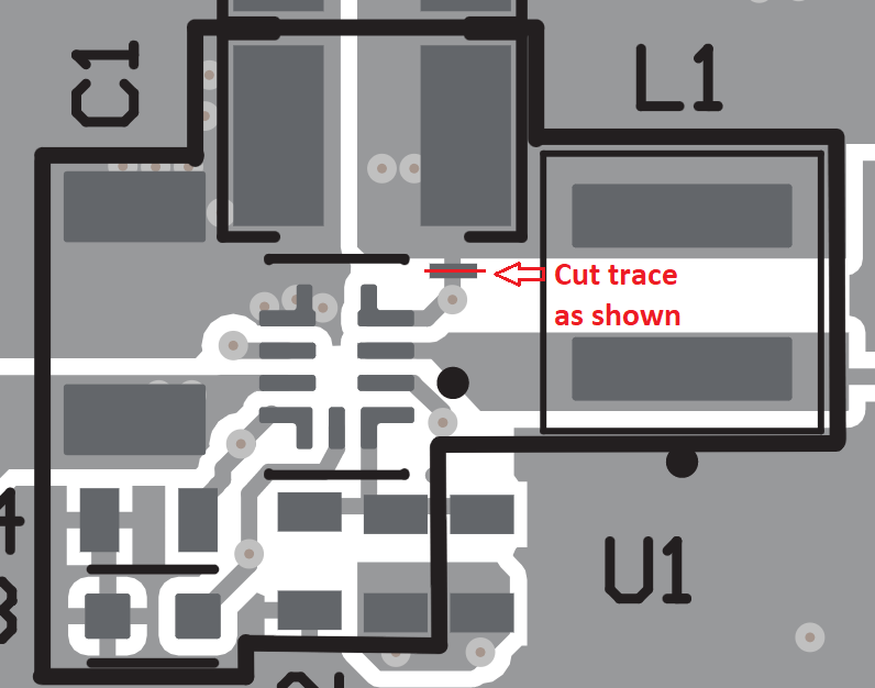
The loop response can be measured with simple changes to the circuitry. First, install a 10-Ω resistor across the pads of R9 on the back of the PCB. The pads are spaced to allow installation of an 0603-sized resistor. Next, cut the short section of trace on the top layer between the via on pin 3 and C2. Figure 1-1 shows this change. With these changes, an AC signal (10-mV, peak-to-peak amplitude recommended) can be injected into the control loop across the added 10-Ω resistor. Figure 4-2 shows the results of this test.
 Figure 1-1 Loop
Response Measurement Modification (Top Layer)