SPRAC76G November 2022 – February 2024 AM5706 , AM5708 , AM5716 , AM5718 , AM5726 , AM5728 , AM5729 , AM5746 , AM5748 , AM5749 , AM620-Q1 , AM623 , AM625 , AM625-Q1 , AM625SIP , AM6411 , AM6412 , AM6421 , AM6422 , AM6441 , AM6442 , AM6526 , AM6528 , AM6546 , AM6548
- 1
- Sitara Processor Power Distribution Networks: Implementation and Analysis
- Trademarks
- 1Introduction
- 2Guidelines for PCB Stack-Up
- 3Physical Layout Optimization of the PDN
- 4Static PDN Analysis (IR Drop Optimization)
- 5Dynamic Analysis of PCB PDN
- 6Checklist for PDN
- 7Implementation Examples and PDN Targets
- Revision History
7.6 AM62xx


Table 7-6 AM62xx PDN Targets and
Decoupling Example
| Supply Name (10) (11) | Static PDN Target | Dynamic PDN Targets | Number of Decoupling Capacitors Per Supply (1) (2)(3) (4) (5) (6) (9) | |||||
|---|---|---|---|---|---|---|---|---|
| Max Reff (mΩ) (7) | Frequency of Interest (MHz) | Dec. Cap. Max LL (nH) (6) (8) | ZTARGET (mΩ) | 0.1 µF | 1 µF | 4.7 µF | 10 µF | |
| VDD_CORE | 23 | ≤1 | 1.5 | 23 | 17 | 1 | 1 | 1 |
| 1-20 | 31 | |||||||
| 20-50 | 35 | |||||||
| VDDS_DDR | For more information, see AM62x DDR Board Design and Layout Guidelines. | |||||||
- For more information on peak-to-peak noise values, see the Recommended Operating Conditions table in the device-specific data manual.
- Loop ESL (excluding the intrinsic decap ESL) from the capacitor pads to the SoC BGA must be as low as possible and not exceed 1.5 nH.
- The Power Delivery Network (PDN) impedance characteristics are defined versus the device activity (that runs at different frequency) based on the Recommended Operating Conditions table of the Specifications chapter of the device-specific processor data manual.
- The static drop requirement drives the maximum acceptable PCB resistance between the PMIC or the external SMPS and the processor power balls.
- This assumes that the external SMPS (power IC) feedback sense is located very close to processor power balls.
- High-frequency (30 MHz to 70 MHz) PCB decoupling capacitors.
- Maximum Reff from VRM/SMPS/PMIC to Processor.
- Maximum Loop Inductance for decoupling capacitor when placed underneath processor BGA.
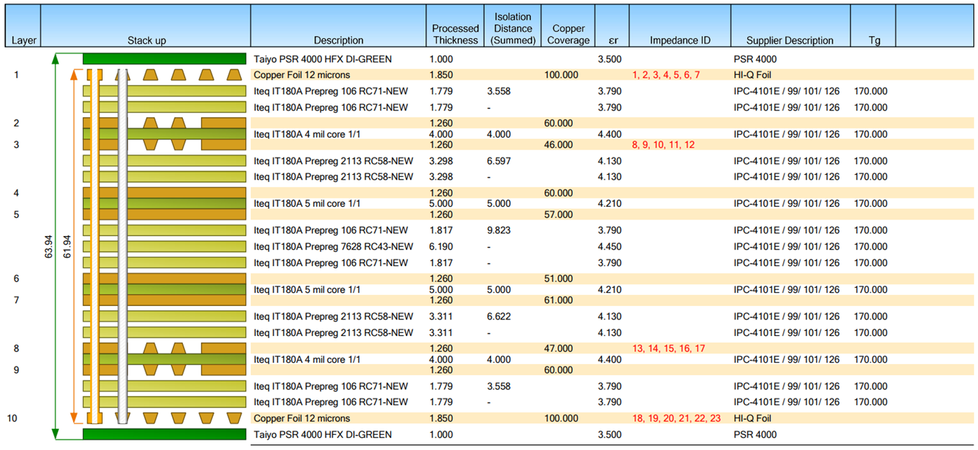
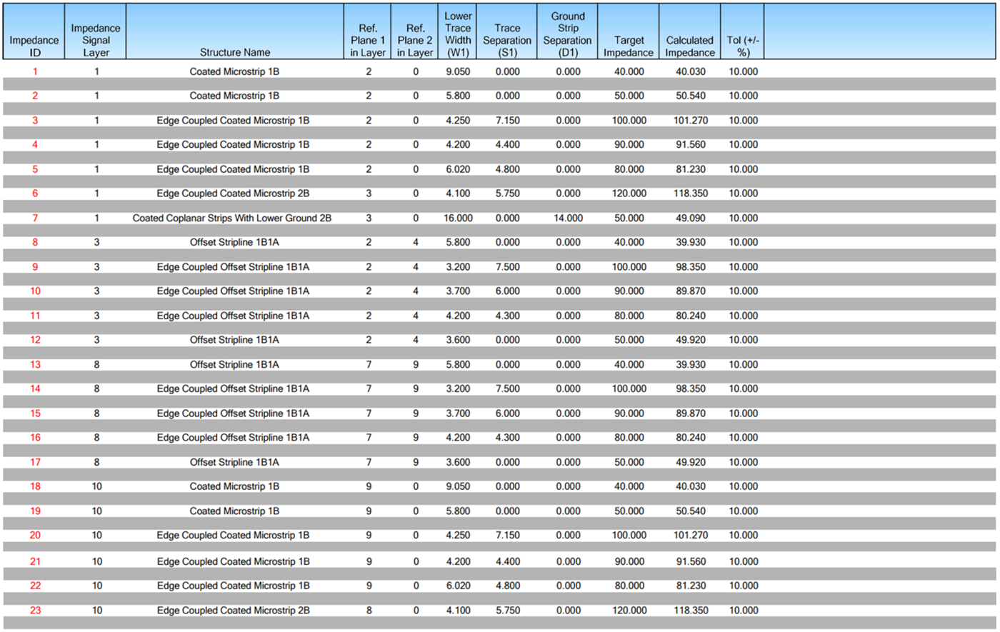
- The decoupling capacitor counts and values presented here are provided as a baseline recommendation only and are based on a specific PCB design. TI recommends that all PCB designs be simulated prior to fabrication to ensure that all processor PDN requirements are met.
- Ganged rails must meet all requirements of each member rail.
- Rails not listed in this table are not simulated by TI due to low load transients. For more information, see the device-specific EVM layout for example implementation of these rails.