SPRACP4A December 2019 – June 2024 AM67 , AM67A , AM68 , AM68A , AM69 , AM69A , DRA821U , DRA821U-Q1 , DRA829J , DRA829J-Q1 , DRA829V , DRA829V-Q1 , TDA4AEN-Q1 , TDA4AH-Q1 , TDA4AL-Q1 , TDA4AP-Q1 , TDA4VE-Q1 , TDA4VEN-Q1 , TDA4VH-Q1 , TDA4VL-Q1 , TDA4VM , TDA4VM-Q1 , TDA4VP-Q1
- 1
- Abstract
- Trademarks
- 1Introduction
-
2High-Speed Interface Design Guidance
- 2.1 Trace Impedance
- 2.2 Trace Lengths
- 2.3 Differential Signal Length Matching
- 2.4 Signal Reference Planes
- 2.5 Differential Signal Spacing
- 2.6 Additional Differential Signal Rules
- 2.7 Symmetry in the Differential Pairs
- 2.8 Connectors and Receptacles
- 2.9 Via Discontinuity Mitigation
- 2.10 Back-Drill Via Stubs
- 2.11 Via Anti-Pad Diameter
- 2.12 Equalize Via Count
- 2.13 Surface-Mount Device Pad Discontinuity Mitigation
- 2.14 Signal Bending
- 2.15 ESD and EMI Considerations
- 2.16 ESD and EMI Layout Rules
- 3Interface-Specific Design Guidance
- 4Board Design Simulations
- 5References
- 6Revision History
2.4 Signal Reference Planes
An electrical circuit must always be a closed loop system. With DC, the return current takes the way back with the lowest resistance for DC signals. At higher frequencies, the return current flows along the lowest impedance path, this lowest impedance path is usually the reference plane adjacent to the signal. For this reason it is always best to have a ground plane or power plane on the layer above or below a signal layer. This solid return path helps to reduce impedance changes and decrease EMI issues.
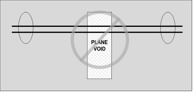
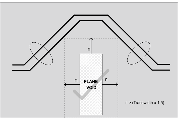
High-speed signals should be routed over a solid GND reference plane and not across a plane split or a void in the reference plane unless absolutely necessary. TI does not recommend high-speed signal references to power planes.
Routing across a plane split or a void in the reference plane forces return high-frequency current to flow around the split or void. This can result in the following conditions:
- Excess radiated emissions from an unbalanced current flow
- Delays in signal propagation delays due to increased series inductance
- Interference with adjacent signals
- Degraded signal integrity (that is, more jitter and reduced signal amplitude)
For examples of correct and incorrect plane void routing, see Figure 2-2 and Figure 2-3.
 Figure 2-2 Incorrect
Plane Void Routing
 Figure 2-3 Correct
Plane Void Routing
Figure 2-3 Correct
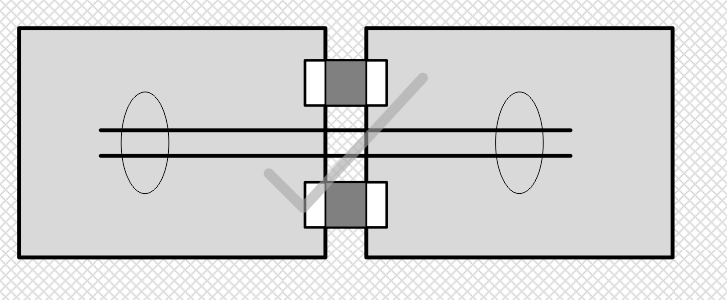
Plane Void RoutingIf routing over a plane-split is completely unavoidable, place stitching capacitors across the split to provide a return path for the high-frequency current. These stitching capacitors minimize the current loop area and any impedance discontinuity created by crossing the split. These capacitors should be 1µF or lower and placed as close as possible to the plane crossing. For examples of incorrect plane-split routing and correct stitch capacitor placement, see Figure 2-4 and Figure 2-5.
 Figure 2-4 Incorrect
Plane-Split Signal Routing
 Figure 2-5 Stitching
Capacitor Placement
Figure 2-5 Stitching
Capacitor PlacementWhen planning a PCB stackup, make sure that planes that do not reference each other are not overlapped because this produces unwanted capacitance between the overlapping areas. To see an example of how this capacitance can pass RF emissions from one plane to the other, see Figure 2-6.
 Figure 2-6 Overlapped Planes
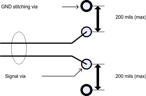
The entirety of any high-speed signal trace should maintain the same GND reference from origination to termination. If unable to maintain the same GND reference, via-stitch both GND planes together to provide continuous grounding and uniform impedance. Place these stitching vias symmetrically within 200mils (center-to-center, closer is better) of the signal transition vias. For an example of stitching vias, see Figure 2-7.
 Figure 2-7 Stitching
Vias
Figure 2-7 Stitching
ViasTI does not recommend high-speed signal references to power planes unless it is completely unavoidable. If it is unavoidable it is best to use AC coupling capacitors and ground vias to allow the return signal to have a path back from the sink to the source.